Sidewinder-100 Board Components
Fig. 8 shows the Sidewinder-100 board component locations, with each numbered component keyed to Table 1.

Fig. 8 Sidewinder-100 Board Components.
| Callout | Ref. Des. | Feature/Component | Notes | Schematic Page Number |
|---|---|---|---|---|
| 1 | U1 | Zynq UltraScale+ XCZU19EG MPSoC with fan sink | Xilinx XCZU19EG-FFVC1760 | |
| 2 | J106 | PS 16 GB DDR4 Memory Lower Bank | Micron MTA18ASF2G72HZ-2G3 | 8 |
| 3 | J107 | PL 16 GB DDR4 Memory Upper Bank | Micron MTA18ASF2G72HZ-2G3 | 9 |
| 4 | J1 | PCIe ×16 Endpoint Connector | only ×8 electrically | 3 |
| 5 | J100 | PCIe ×8 Host Socket | mutually exclusive with NVMe 1 | 21 |
| 6 | J113 | U.2 Port NVMe 0 | powered at bootup | 20 |
| 7 | J113 | U.2 Port NVMe 1 | mutually exclusive with PCIe ×8 Host | 20 |
| 8 | J110 | M.2 Card Slots NVMe 2 | 20 | |
| 9 | J111 | M.2 Card Slots NVMe 3 | 20 | |
| 10 | J8 | QSFP28 0 | 21 | |
| 11 | J9 | QSFP28 1 | 21 | |
| 12 | J2 | ATX PCIe Power Connector | 3 | |
| 13 | J33 | USB to Dual UART Bridge | Silicon Labs CP2105 | 12 |
| 14 | J104 | JTAG Connector | 4 | |
| 15 | J117 | Management Ethernet GEM 3 | Microchip KSZ9031RNXCC | 5 |
| 16 | U114 | PCIe Clock Chip | IDT 9DBL0841BKILF | 16 |
| 17 | U115 | NVMe Clock Chip | IDT 9FGL0841BKILF | 17 |
| 18 | U117 | QSFP Clock Chip (322,265 MHz by default) | IDT 8T49N240-002NLGI | 18 |
| 19 | U133 | PL DDR4 Clock Chip (333,33 MHz by default) | IDT 9FGV1004B200NBGI | 19 |
| 20 | U116 | Reference Clock Chip (33,33 MHz PS, 100/200 MHz PL by default) | IDT 9FGV1004B201NBGI | 19 |
| 21 | J114 | PCIe Spread Spectrum Clock Selection Jumper | open by default | 17 |
| 22 | J119 | Brute Force Clock Programming Jumper | open by default | 16 |
| 23 | U75, U76 | 256 MB QSPI Flash | Micron MT25QL01GBBA8E12-0SIT | 5 |
| 24 | J102 | Micro SD Card Slot SD 1 | 5 | |
| 25 | D53-55 | 3× User LEDs | Actice-High | 11 |
| 26 | SW11-13 | 3× User Pushbutton Switches | Active-Low | 11 |
| 27 | SW5 | Boot Mode DIP Switch | JTAG, QSPI, SD | 4 |
| 28 | SW8-10 | Reset Pushbutton Switches | 4 | |
| 29 | D1, D37-39, D44-52 | Status LEDs | Power Rails, PS Error and Status | |
| 30 | D36 | Reset LED (see Status LEDs) | 4 | |
| 31 | D42 | NVMe 2 Drive Activity LED | 20 | |
| 32 | D43 | NVMe 3 Drive Activity LED | 20 |
Zynq UltraScale+ XCZU19EG MPSoC
The Sidewinder-100 board is populated with the Zynq UltraScale+ XCZU19EG-FFVC1760 MPSoC, which combines a processing system (PS) and programmable logic (PL) into a single device. Revision 2 of the Sidewinder-100 is shipped with a ES 2, temperature grade I and -2 speed grade device.
Clock Generation
Multiple Clocks are fed to the FPGA to drive the different interfaces. Most are dedicated to specific interfaces and their default rates are setup accordingly, such as the 322.25625 MHz for the Ethernet interfaces conencted to the respective QTY transceiver reference clock inputs. Fig. 9 shows the clocks connected to the FPGAs.
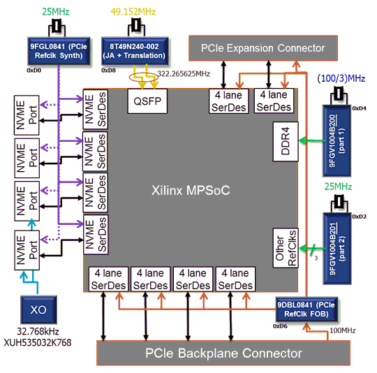
Fig. 9 Clock Generation
Additionally two general purpose clocks are connected to FPGA fabric clock capable pins, one 100 MHz and one 200 MHz clock.
High-Speed Transceiver Bank Usage
The XCZU19EG FPGA provides two types of transceivers, namely GTY and GTH. The transceivers are organized in quads, each comprising four transceiver pairs and two reference clock inputs as well as dedicated PLLs. Fig. 10 shows the transceiver bank layout and the functions using the respecitve transceiver quads.

Fig. 10 Bank Diagram.
PS 16 GB DDR4 Memory
The PS-side lower memory slot is wired to the Zynq UltraScale+ MPSoC DDR memory controller. The Sidewinder-100 is shipped with a DDR4 ECC SDRAM SODIMM of type Micron MTA18ASF2G72HZ-2G3, which adheres to the JESD21-C label 16 GB 2R×8 PC4-2400T-TH0-11. Due to restrictions of the MPSoC memory PHY regarding dual-rank DIMMs, it can only be driven with a maximum data rate of 1866 MB/s.
PL 16 GB DDR4 Memory
The PL-side upper memory slot is wired to banks 64, 65 66 of the XCZU19EG FPGA. The Sidewinder-100 is shipped with a DDR4 ECC SDRAM SODIMM of type Micron MTA18ASF2G72HZ-2G3, which adheres to the JESD21-C label 16 GB 2R×8 PC4-2400T-TH0-11. Due to restrictions of the MPSoC memory PHY regarding dual-rank DIMMs, it can only be driven with a maximum data rate of 1866 MB/s.
PCIe ×16 Endpoint
The PCIe device interface provides a Generation 3 x16 connection to a host connected via the PCB edge connector, see callout 4 in Fig. 8 and Table 1. The host interface is connected via two GTH quads 224 - 227 (X0Y0 - X0Y3). The needed 100MHz reference clock is supplied to the FPGA via the PCB edge connector.
PCIe ×8 Host
The PCIe host interface provides a Generation 3 x8 connection to endpoints connected to the edge socket, see callout 5 in Fig. 8 and Table 1. The host interface is connected via two GTH quads 230, 231 (X0Y6, X0Y7). The needed 100MHz reference clock is supplied on the board to the socket and the FPGA.
Please note that the power supply to the host socket has to be switched on by software running on the PS.
M.2 Card Slots
The board features two M.2 Card slots conencted, see callout 8 and 9 in Fig. 8 and Table 1. Each M.2 card slot provide two PCIe Gen3 x5 interface, e.g. for NVMe disks, connected to a separate GTY transceiver. M.2 slot NVMe2 is connected to transceiver quad 128 (X0Y1). M.2 slot NVMe3 is connected to transceiver quad 127 (X0Y2). The needed 100MHz reference clock is supplied on the board to the connectors and the FPGA.
JTAG Connector

Fig. 11 JTAG Connector Pin Assignment. Numbers in braces denote callout in Fig. 8.
Fig. 11 shows the pin assignment and relative position of the JTAG connector, which is wired to the JTAG chain of the Zynq UltraScale+ MPSoC.
USB to Dual UART Bridge
The USB to Dual UART Bridge of type Silicon Labs CP2105 provides two level-shifted UART connections through the Micro USB connector J33. Both channels are wired to the PS MIO.
QSFP28 Connectors
The two QSFP28 connectors provide Ethernet connectivity for up to 100 GBit/s each, see callout 10, 11 in Fig. 8 and Table 1. Each connecter supports 40 GbE or 4x 10 GbE or 4x 25 GbE or 2x50 GbE connectivity. QSFP28 0 is connected to GTY transceiver quad 130 (X0Y3). QSFP28 1 is connected to GTY transceiver quad 131 (X0Y4). The needed reference clock is supplied by the board. It is configured to 322.265625 MHz, which is suitable for Ethernet protocols
Please note that the power supply to the host socket has to be switched on by software running on the PS.
Management Ethernet
This section shows how to connect the Ethernet management interface of the board. This differs for the respecitve hardware revisions, each targetted in their respecitve subsections.
Hardware Revision 2.0
For the Sidewinder-100 Hardware Revision 2.0, the PS-side 10/100/1000 MB/s GEM 3 is connected to a Microchip KSZ9031RNXCC Ethernet RGMII PHY before being routed to pin header J117. In order to use the management ethernet port, one needs to attach the accompanying off-board RJ45 connector adapter cable with magnetics to pin header J117. The adapter cable is correctly aligned if it points towards the PCIe ×8 host connector, away from the board.

Fig. 12 RJ45 connector adapter cable LEDs.
| Pin | Purpose | Description |
|---|---|---|
| LED1 | Activity | Blinks green if there is data flowing, otherwise off. |
| LED2 | Link | Turns green if the link is up, otherwise off. |
There are two green LEDs embedded into the RJ45 connector. Their positions and purposes are shown in Fig. 12, while Table 2 shows their meaning.
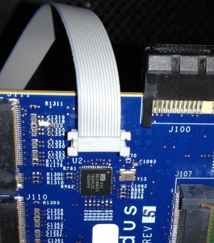
Fig. 13 Connection of the RJ45 adapter cable
Status LEDs

Fig. 15 Status LEDs board location.
| Ref. Des. | Purpose | Description |
|---|---|---|
| D1 | PS INIT | Indicates the PS is initialized after a power-on reset (POR). (GRN/RED)? |
| D36 | PS RESET | Indicates PS reset. |
| D37 | PS DONE | Indicates the PL configuration is completed. |
| D38 | PS ERROR OUT | Signal is asserted for accidental loss of power, an error, or an exception in the PMU. |
| D39 | PS ERROR STATUS | Indicates a secure lockdown state. Alternatively, it can be used by the PMU firmware to indicate system status. |
| D44 | 0V85 | 0,85 V rail power-good |
| D45 | 1V8 | 1,8 V rail power-good |
| D46 | 1V2 | 1,2 V rail power-good |
| D47 | 12 V ATX | 12 V ATX PCIe connector input power |
| D48 | 12 V PCIe | 12 V PCIe edge connector input power |
| D49 | 3V3 PCIe | 3,3 V PCIe edge connecter input power |
| D50 | 0V9 | 0,9 V rail power-good |
| D51 | 5V8 | 5,8 V rail power-good |
| D52 | 3V3 | 3,3 V rail power-good |
Fig. 15 shows the status LEDs of the Sidewinder-100, which can be found on the back side of the board on the upper corner adjacent to the ATX cage. Table 3 describes these LEDs in more detail.
Reset Pushbutton Switches
| Ref. Des. | Purpose | Description |
|---|---|---|
| SW8 | PS PROG | PL configuration reset signal. |
| SW9 | PS SYSTEM RESET | System reset commonly used during debug. |
| SW10 | PS POWER ON RESET | Power-on reset signal. |
Table 4 describes the reset pushbutton switches, which can be found on the back side of the board on the upper corner adjacent to the ATX cage.
Boot Mode

Fig. 16 Boot Mode DIP Switch set to SD card.
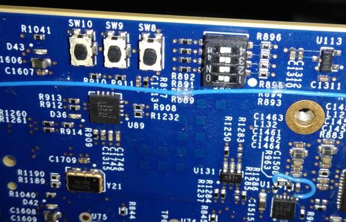
Fig. 17 Switch location and orientation on the board.
| Boot Mode | Mode SW5 |
|---|---|
| JTAG | on, on, on, on |
| QSPI24 | off, on, on, on |
| QSPI32 | on, off, on, on |
| SD1 | off, on, off, on |
Fig. 16 shows the location of the boot mode DIP switch, while Table 5 lists the boot modes and their respective switch settings.