PCIe Endpoint Example Design
This section describes how to build and re-compile the PCIe Endpoint Example Design of the ZU19SN Reference Design.
This PCIe Endpoint Reference design is delivered as build scripts as well as pre-built SD card images. The design implements a PCIe Endpoint with vendor ID 0x10ee and device ID 9031. It exposes multiple base address registers (BARs) to the host, each providing a separate and independent interface within the FPGA.
- BAR0 implements a PCIe AXI bridge corresponding to an AXI-light interface.
- BAR1 implements a DMA channel corresponding to a pair of AXI-S interaces, which are not used in this example.
- BAR2 implements a PCIe AXI bridge corresponding to an AXI-MMAP interface.
For testing the PCIe Endpoint design plug the board into a PCIe x16 slot of a PC mainboard and connect the additional power supply socket. Boot the PC, which will not recognize the PCIe device yet, because the time needed to configure the FPGA according to the SD-Card images is too long for the BIOS to discover the device. Reboot the PC and make sure the PCIe devices are not repowered, so that the BIOS and Linux discover the PCIe device.
Make sure the host runs a Linux, e.g. Ubuntu 16.04 and has a gcc toolchain and make installed to build the test tool.
Build Bitfile
First make sure to load the Xilinx Vivado 2016.4 environment, e.g. by sourcing the appropriate shell scripts provided by Xilinx, e.g. /opt/xilinx/vivado/v2016.4/Vivado/2016.4/settings64.sh.
Afterwards additionally load the Xilinx PetaLinux 2016.4 environment, e.g. via the shell scripts provided by Xilinx, e.g. /opt/xilinx/petalinux/v2016.4/settings.sh.
Now change into the pl directory and build the PL design part via a bunch of bash and tcl scripts executed by vivado:
# ./build.sh pcie_ep
Note
Since the Sidewinder-100 in Rev.2 uses an engineering sample (ES) FPGA, please ensure that you configured Vivado to support beta devices by adding enable_beta_device* to your configuration, which might you local user configuration being located at ~/.Xilinx/Vivado/init.tcl.
For more information about the init.tcl file refer to this link in the Vivado Design Suite Tcl Command Reference Guide (UG835).
The build itself is executed in a dedicated folder within the scripts/run/ path in the pl directory.
The name of the build directory contains the build name and a timestamp, e.g. pcie_ep_build_20170715-153953.
This ensures that multiple builds do not interfere with each other.
When the build process finishes the bitfile is ready and available in the subdirectory scripts/run/pcie_ep_build_20170715-153953/pcie_ep_fpga_design.runs/impl_1/fpga_top.bit.
As another build result a vivado project is available scripts/run/pcie_ep_build_20170715-153953/pcie_ep_fpga_design.xpr.
The system ILA cores providing insight into the hardware system and the AXI transaction corresponding to the PCIe transaction are built into the project.
Build PetaLinux
In order to include the generated debug bitfile into the SD card image, build a petalinux project as described in section PetaLinux until reaching step SD Card. When this step is reached, reset the environment variable for the bitfile to be included into the SD card image to point to the recently generated debug bitfile and go on with building the petalinux image:
# export BITSTREAM=../../pl/scripts/run/pcie_ep_build_20170715-153953/pcie_ep_fpga_design.runs/impl_1/fpga_top.bit
# make package-boot
Afterwards the petalinux images are ready to be copied to the SD card and the Fidus board can be booted with them.
Build Host Software
To test the hardware, a set of software tools and scripts is used.
The tools are located in the sw/pcie_ep folder.
To compile the pcimem tool, change to the sw/pcie_ep/pcimem folder and type make:
# make
gcc -Wall -g    pcimem.c   -o pcimem
The pcimem tool allows to access the BARs directly via the command line at a given address.
Debug Hardware
The embedded ILA cores are attached to the internal AXI interfaces attached to the PCIe Endpoint. The hardware is regularly build with debug cores in it. These debug cores are system ILA cores attached to the AXI interfaces, which are mapped to a BAR each respectively as described in section PCIe Endpoint Example Design.
The trigger is best configured to a global OR and each available valid flags of the various channels equal to 1.
All ILA system cores are setup the same way accordingly, see also Fig. 23.
Engage all triggers prior to executing the test script pcie_ep_test.sh.
Then execute the testscript pcie_ep_test.sh from within the folder sw/pcie_ep:
# cd sw/pcie_ep
# sudo ./pcie_ep_test.sh

PCI_DEVICE:    0000:05:00.0
PCI_VENDOR_ID: 10ee
PCI_DEVICE_ID: 9031

Testing BARs
  BAR 0 at f7c10000 of size 16384
  BAR 2 at f7c14000 of size 16384

Check BAR 0 of size 16384 using /sys/bus/pci/devices/0000:05:00.0/resource0 for pre-initialization
memory region of BAR 0 is all zeros

Check BAR 2 of size 16384 using /sys/bus/pci/devices/0000:05:00.0/resource2 for pre-initialization
memory region of BAR 2 is all zeros

Start read write test on BAR 0 at offset 0...
Write and read back on memory region of BAR 0 was successfull

Start read write test on BAR 2 at offset 0...
Write and read back on memory region of BAR 2 was successfull
Note
You might need to enforce the execution within a bash shell instead of other system shells, which is indicated e.g. by the following output:
./pcie_ep_test.sh: 48: ./pcie_ep_test.sh: Syntax error: "(" unexpected
To enforce the execution by the bash shell, use the following modified command line:
# sudo bash -c ./pcie_ep_test.sh
During the phases of testing (read and read/write/read) of the BARs respectively, the access pattern noticable on the AXI interfaces change. Fig. 23 shows the read access pattern, while Fig. 24 shows the read/write/read access pattern of the AXI light interface mapped to BAR0. Fig. 25 shows the read access pattern, while Fig. 26 shows the read/write/read access pattern of the AXI memory mapped (MM) interface mapped to BAR2. Fig. 27 provides a more detailed view into the read/write/read pattern access on the AXI-MM interface of BAR2.
The AXI streaming (S) interface mapped to BAR1 is not yet used as the corresponding DMA interface has not yet been added to the software.
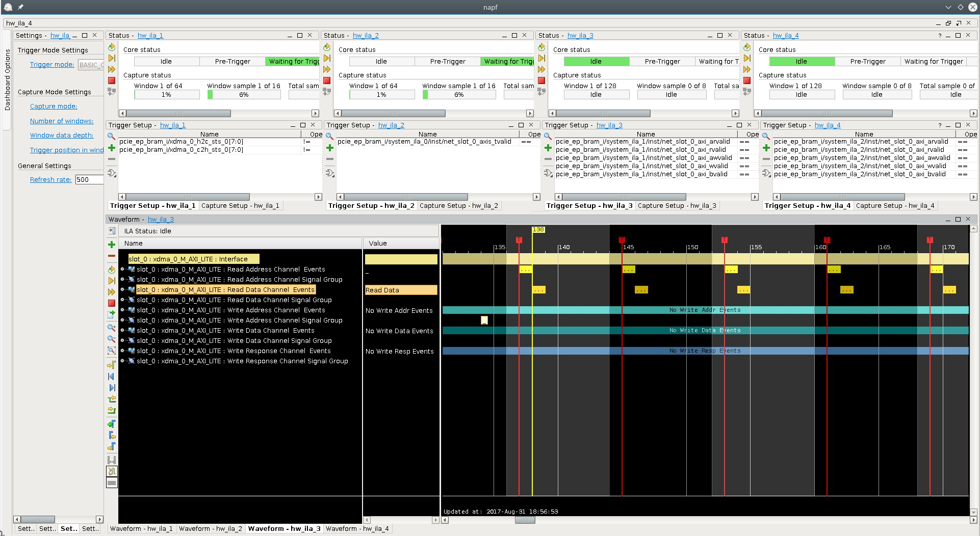
Fig. 23 Chipscope image of BAR0 AXI interface during PCIe read access
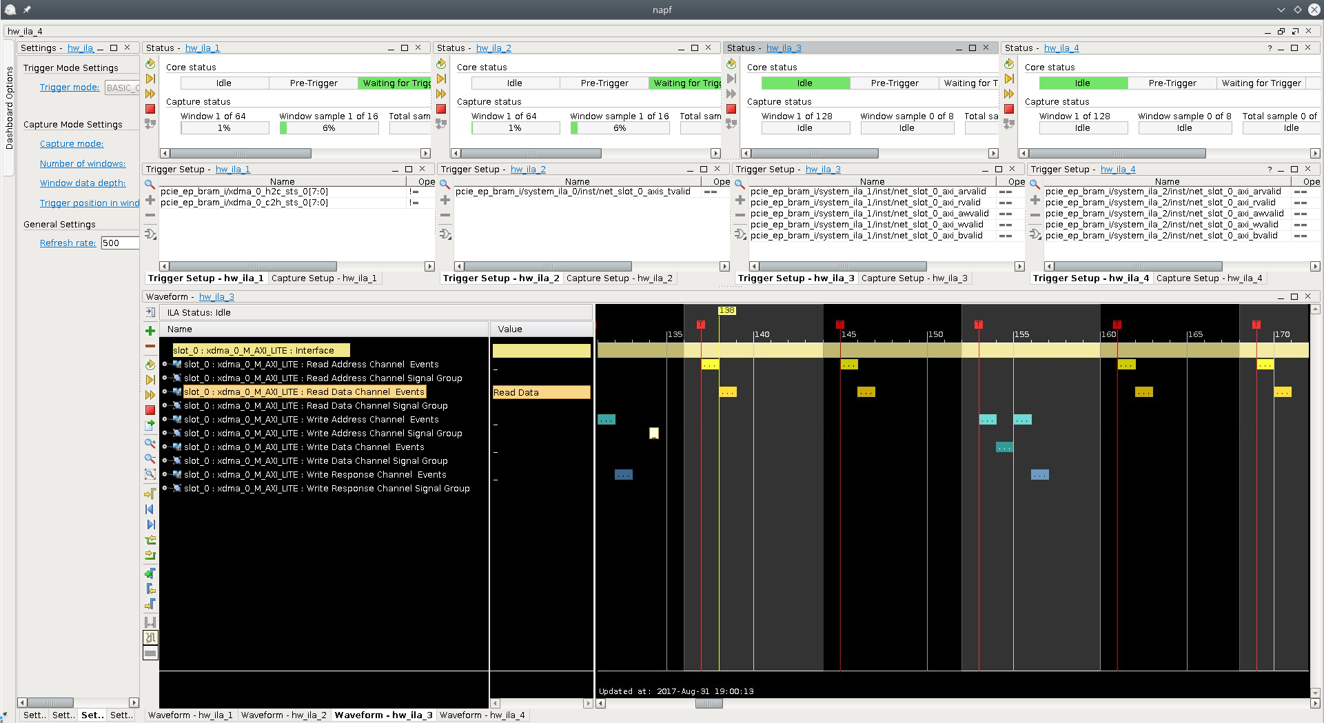
Fig. 24 Chipscope image of BAR0 AXI interface during PCIe read/write/read access
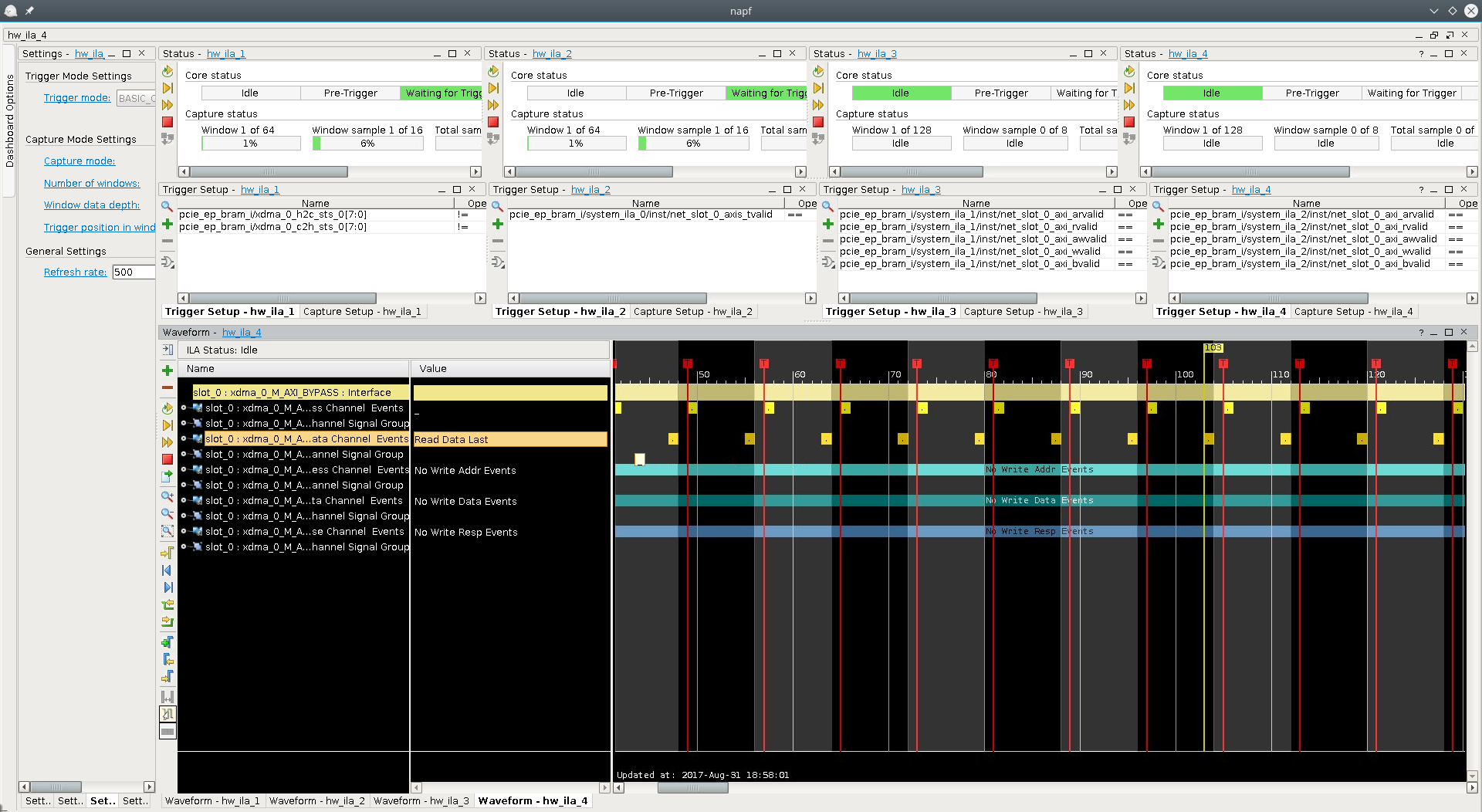
Fig. 25 Chipscope image of BAR2 AXI interface during PCIe read access
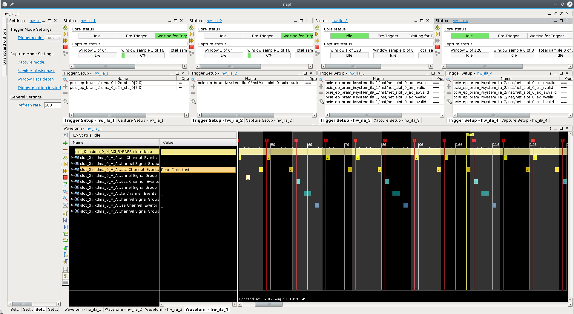
Fig. 26 Chipscope image of BAR2 AXI interface during PCIe read/write/read access
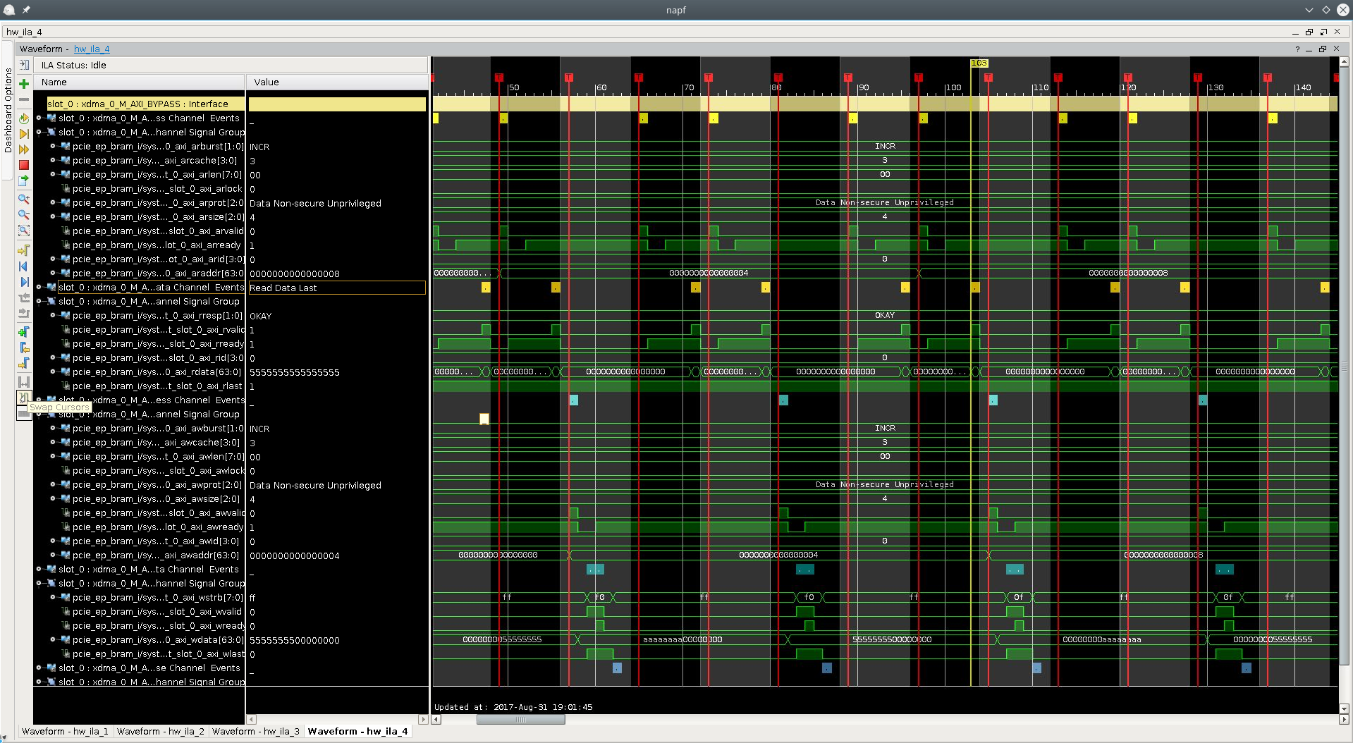
Fig. 27 Chipscope image of BAR2 AXI interface during PCIe read/write/read access
Compatibility
PCIe is a standard maintained by the PCI SIG. To proove compliance and interoperability each PCI and PCIe device needs to successfully pass a plugfest. However, due to the complexity of the technology glitches occur for specific combinations of devices.
We tested the a Rev. 2 board and the provided design with the following CPUs and Mainboards:
- First Setup (x16 Gen 3 Link)
- Ubuntu 14.04
- H110I PRO (MS-7995) version 1.0 Mainboard
- Firmware Revision 3.80
- 2x 4 GiB RAM F4-2133C15-4GNT
- Intel i3-6100T CPU @ 3.2 GHz, comprising a Sky Lake PCIe Controller
- Board attached to PCIe slot 1
- Second Setup (x8/4 Gen 2 Link)
- Ubuntu 16.04
- Z77A-G43 (MS-7758) version 1.0
- Firmware Revision V2.1
- 2x 4 GiB RAM KHX1600C9D3/4GX
- Intel i5-3450S CPU @ 2.80GHz, comprising 7 Series/C210 Series Chipset Family PCI Express Root Port 1, 2
- Board attached to PCIe slot e1 (PEG port) (no link)
- Board attached to PCIe slot e4 (x4 Gen2)
If you encounter interoperability issues with the provided board and design, please provide the output of the sudo lshw -sanitize.
References
For further information you may have a look at the following documents and tools: