10/25 GbE MAC Loopback Example Design
This section describes how to build and re-compile the 10/25 GbE MAC Loopback Example Design of the ZU19SN Reference Design.
This MAC Loopback Reference design is delivered as build scripts, as the 10/25 GbE MAC available for the Zynq UltraScale+ from Xilinx is a core which requires a separate license to be aquired from Xilinx. This guide walks through the process of building the Ethernet MAC Loopback reference design for the Fidus Sidewinder 100 board on a high level, focussed on design flow steps specific to this project.
The build process of the 10 GbE and 25 GbE MAC Loopback Reference Design are the same, just the design names and IP configuration differ. So, the following steps may both be used for 10 GbE and 25 GbE reference designs.
Note
Please note that in order to use the QSFP Ethernet connectors present on the board, the power supply for these interfaces need to be switched on by software running on the PS. So it is necessary to use some piece of software to switch it on initially. This is taken care of by the PetaLinux system provided along with this example design, see PetaLinux. Afterwards you may reconfigure the FPGA part.
Build Bitfile
First make sure to load the Xilinx Vivado 2016.4 environment, e.g. by sourcing the appropriate shell scripts provided by Xilinx, e.g. /opt/xilinx/vivado/v2016.4/Vivado/2016.4/settings64.sh.
Afterwards additionally load the Xilinx PetaLinux 2016.4 environment, e.g. via the shell scripts provided by Xilinx, e.g. /opt/xilinx/petalinux/v2016.4/settings.sh.
Now change into the pl directory and build the PL design part via a bunch of bash and tcl scripts executed by vivado (10 GbE):
# ./build.sh mac_lb_10g
(25 GbE):
# ./build.sh mac_lb_25g
Note
Since the Sidewinder-100 in Rev.2 uses an engineering sample (ES) FPGA, please ensure that you configured Vivado to support beta devices by adding enable_beta_device* to your configuration, which might you local user configuration being located at ~/.Xilinx/Vivado/init.tcl.
For more information about the init.tcl file refer to this link in the Vivado Design Suite Tcl Command Reference Guide (UG835).
The build itself is executed in a dedicated folder within the scripts/run/ path in the pl directory.
The name of the build directory contains the build name and a timestamp, e.g. mac_lb_10g_build_20170715-153953.
This ensures that multiple builds do not interfere with each other.
When the build process finishes the bitfile is ready and available in the subdirectory scripts/run/mac_lb_10g_build_20170715-153953/mac_lb_10g_fpga_design.runs/impl_1/fpga_top.bit.
As another build result a vivado project is available scripts/run/mac_lb_10g_build_20170715-153953/mac_lb_10g_fpga_design.xpr, which can be used for setting up a debug version of the design, see Build Debug Bitfile.
Build Debug Bitfile
To build the bitfile with added visibility cores, i.e. Xilinx ChipScope ILA cores, the Vivado project created by the build flow is used. Within the shell with a loaded Vivado environment navigate to the build directory and open the project:
# cd scripts/run/mac_lb_10g_build_20170715-153953/
# vivado mac_lb_10g_fpga_design.xpr
The scripts delivered as part of this reference design already include a set of signals marked to be included in a debug interface.
To include those into the bitfile, click Set Up Debug and follow the wizard for including the debug circuitry into the netlist.
The wizard asks for the number of registers to be inserted into the data pipeline.
To ease timing closure it is good to add about 2-3 register stages.
Afterwards generate a new bitfile.
When the bitfile is ready, it can be downloaded to the FPGA target using JTAG access via Vivados hardware manager or the bitfile can be integrated into the SD card images.
ChipScope can then connect to the debug cores within the running design via JTAG.
Build PetaLinux
In order to include the generated debug bitfile into the SD card image, build a petalinux project as described in section PetaLinux until reaching step SD Card. When this step is reached, reset the environment variable for the bitfile to be included into the SD card image to point to the recently generated debug bitfile and go on with building the petalinux image:
# export BITSTREAM=../../pl/scripts/run/mac_lb_10g_build_20170715-153953/mac_lb_10g_fpga_design.runs/impl_1/fpga_top.bit
# make package-boot
Afterwards the petalinux images are ready to be copied to the SD card and the Fidus board can be booted with them.
Debug Hardware
When the board is started using a bitfile with debug cores built in, traffic flowing through the FPGA may be observed via Xilinx ChipScope.
This is best done by setting the triggers of RX and TX busses on the MAC interface to the valid signals respectively.
The trigger settings as well as the resulting traces are shown in Fig. 21 and Fig. 22 for both directions respectively.
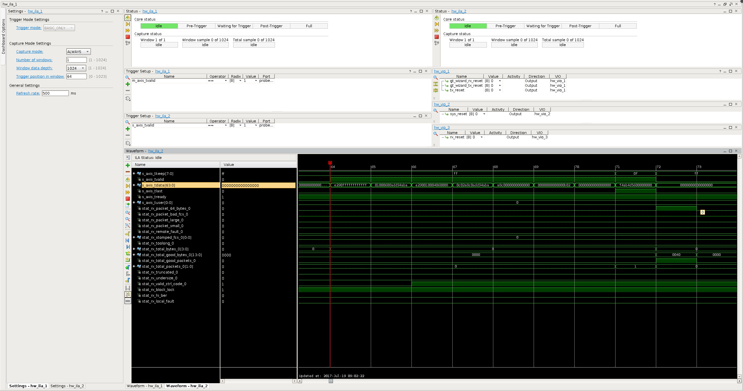
Fig. 21 Chipscope image of RX AXI-S interface
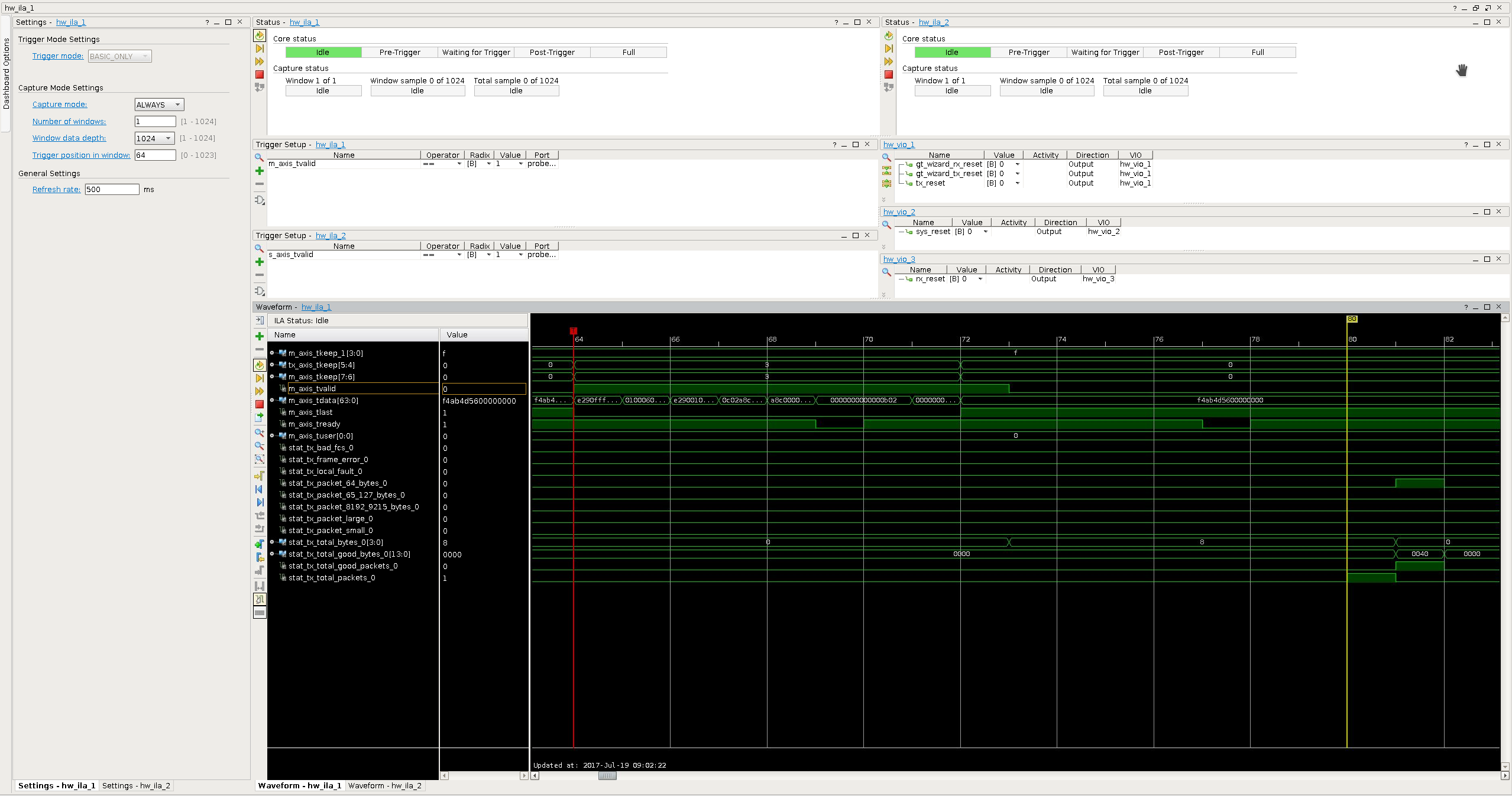
Fig. 22 Chipscope image of TX AXI-S interface
Reset Circuitry
Generally it is not necessary to pull the reset of any part of the 10/25G Ethernet Subsystem. However, the MAC Loopback Design per default includes three Xilinx ChipScope VIO cores, which are generated by the build scripts and instantiated in the top entity of the design. These VIO cores let the user control the various reset signals of the Xilinx 10/25G Ethernet Subsystem.
Each core is driven with the clock associated with the reset signals driven by the VIO core. For further information about resetting the parts of the Ethernet Subsystem, please see Xilinx 10/25 Ethernet Subsystem Product Guide (PG210 v2.0 - as used in the design).
References
For further information you may have a look at the following documents: