A Deep Dive into AMD/Xilinx AXI Bridge for PCI Express (AMD/Xilinx PG194) and Why We Tweaked C_M_AXI_NUM_READQ
Executive Summary
AMD/Xilinx’ AXI Bridge for PCI Express (PG194) implements a bi-directional communication channel from and to FPGA internal memory mapped AXI4 masters and slaves to and from external PCIe connected memory mapped devices, with the FPGA operating as PCIe endpoint or root port.
In many scenarios the performance of forwarding communication between the two protocols, AXI4 and PCIe, is sufficient and the AMD/Xilinx IP core can be used as well. However, in certain cases tweaking is necessary to achieve the expected throughput.
Depending on the amount of extra performance required the modification ranges from simply tuning a hidden parameter to patching the IP’s HDL sources. In the example project used for this description the PCIe peer to peer (P2P) write performance from an FPGA to a 12 NVMe SSD RAID0 increased from 2.700 MiB/s to 4.900 MiB/s to 8.600 MiB/s.
AMD/Xilinx AXI Bridge for PCI Express Overview
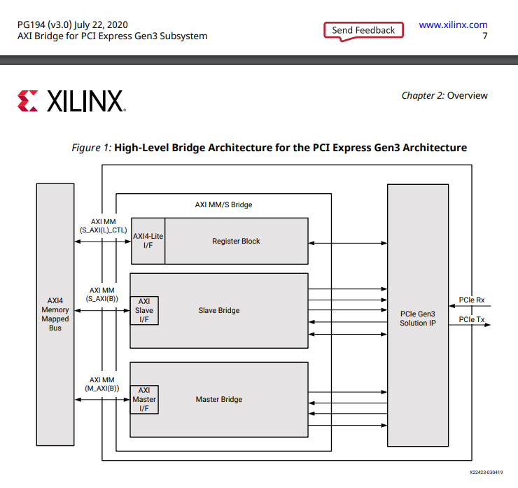
The AMD/Xilinx AXI Bridge for PCI Express is implemented differently for different AMD/Xilinx FPGA families. This description focuses on the “AMD/Xilinx DMA//Bridge Subsystem for PCI Express in AXI Bridge mode” implementation as found in AMD/Xilinx UltraScale+ devices.
The bridge IP core comprises the actual bridging logic, converting PCIe TLPs to AXI4 transactions and vice versa, and a PCIe IP core implementing the physical PCIe interface and forwarding PCIe TLPs via multiple AXI4-Stream interfaces. The PCIe IP core for Ultrascale+ is described in PG213. The bridging logic has two main and distinct blocks, the so-called Slave Bridge and the so-called Master Bridge. The Slave Bridge receives AXI4 memory mapped transactions from FPGA internal AXI4 master IP cores and converts them to PCIe request TLPs, operating as a PCIe bus master or “Requester”. The Master Bridge on the other hand receives PCIe request TLPs as a “Completer” and converts them to AXI4 memory mapped transactions targeting FPGA internal AXI4 slave IP cores.
For this description we will only look at the Master Bridge and specifically only at PCIe read request TLPs resulting in AXI4 reads initiated by the AMD/Xilinx AXI Bridge for PCI Express. The AMD/Xilinx PG213 PCI Express IP interfaces involved are the two AXI4-Stream interfaces CQ (Completer reQuest) and CC (Completer Completion). Remember, for these kinds of transfers the FPGA is the Completer of PCI traffic, and it first receives a PCIe Read Request TLP on CQ, and then responds with a PCIe Completion TLP on CC.
The CQ interface of the AMD/Xilinx PG213 PCIe IP core has some sideband signals independent of the AXI4-Stream interface to handle the flow of TLPs. This is necessary to cope with some of the PCIe ordering rules. Specifically PG213 allows connected logic, the AMD/Xilinx PG194 AXI bridge logic in this case, to hold off any PCIe Read Request TLPs (called non-posted requests or np) and instead receive PCIe Write Request TLPs that arrived at the PCIe core later but can now skip the line and move forward in the receive queue. The AMD/Xilinx PG213 PCIe IP core implements a flow control mechanism at its AXI4-Stream CQ interface to achieve this. This flow control is not to be confused with PCIe flow control, and the credits mentioned in this context are not PCIe flow control credits, although the concept is very similar.
The AXI4-Stream CQ slave, the Master Bridge logic in this case, can provide up to 32 credits for non-posted requests to the AMD/XIlinx PG213 PCIe IP Core. Each non-posted request consumes one credit when sent over the CQ interface. And each assertion of the pcie_cq_np_req two-bit signal grants one or two credits depending on the signal’s value. The AMD/Xilinx PG213 PCIe IP Core maintains an internal counter named pcie_cq_np_req_count to track the number of available credits. As mentioned, each non-posted request decrements the counter and pcie_cq_np_req assertions increment it. The counter can assume values of 0 to 32. If the counter hits 0, no non-posted requests are sent over the CQ interface any more and the AMD/Xilinx PG213 PCIe IP Core instead provides posted requests if available.
Performance Limitations in certain Scenarios
The AMD/Xilinx PG194 Master Bridge by default only provides a maximum of 2 credits for non-posted requests to the AMD/Xilinx PG213 PCIe IP Core. These two credits are initially granted as a baseline and then it seems that there is one credit grant following each non-posted request reception. Since there is latency involved in the loop from request reception to granting the credit to the AMD/Xilinx PG213 incrementing the credit counter and then to finally providing another non-posted request based on the counter update, this basically implements a non-posted request rate limit. In combination with small non-posted requests this can significantly limit the achievable bandwidth. In one example of 12 NVMe SSDs RAID0 reading from the FPGA, bandwidth was limited to 2.700 MiB/s for a PCIe Gen3 x16 link, which is far less than expected in this setup.
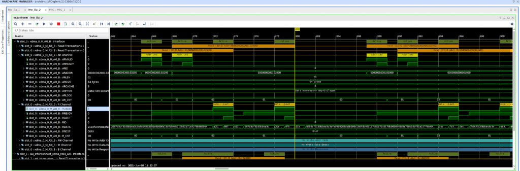
In the below screenshot of the Vivado ILA debugger it can be seen that two read transactions follow each other closely, are then followed by a pause, and then another two close by read transactions. This pattern continues and obviously the AXI4 possible bandwidth (matching the PCIe bandwidth) is not fully utilized.
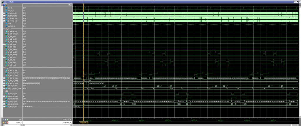
Looking at the simulation of this same setup, the root cause can be seen. The AMD/Xilinx PG194 Master Bridge tries to maintain a pcie_cq_np_req credit level of 2, as mentioned above. These two credits are rapidly consumed by two consecutive PCIe non-posted read requests. After receiving each of them the AMD/Xilinx PG194 Master Bridge grants a new credit soon thereafter by asserting pcie_cq_np_req, but the latency of the path described above until the next request is provided is just too high to prevent a long pause. The pcie_cq_np_req_counter drops to 0 and transfers are throttled.
The setting defining the pcie_cq_np_req credit level initially granted and maintained by the AMD/Xilinx PG194 Master Bridge is configured by the hidden AMD/Xilinx PG194 configuration parameter C_M_AXI_NUM_READQ (not to be confused with C_M_AXI_NUM_READ). As mentioned, it defaults to 2. This is also the only value officially supported by AMD/Xilinx (which is why the parameter is hidden). However, one other value, 4, can be set via TCL. Doing so bumps the NVMe SSD RAID0 bandwidth to 4.900 MiB/s.
set_property CONFIG.C_M_AXI_NUM_READQ 4 [get_ips xdma_0]A further increment is not possible via TCL. Instead, the HDL has to be patched to use a value outside the TCL allowed range. An increment to 8 increased the bandwidth of our example setup to 8.600 MiB/s, which is very close to the expected, as the pattern generator providing the SSDs DMA data is limited to 9.000 MiB/s.
set hdl_synth_top \

[get_files -all -used_in synthesis \

-compile_order sources \

-of [get_ips xdma_0] xdma_0.sv]

package require fileutil

::fileutil::updateInPlace $hdl_synth_top \

[list string map \

[list {.C_M_AXI_NUM_READQ(2),} \

".C_M_AXI_NUM_READQ(8),"]]
Learn more about our capabilities in PCI Express (PCIe) Connectivity to achieve extra performance.
🌐 www.missinglinkelectronics.com
MLE (Missing Link Electronics) is offering technologies and solutions for Domain-Specific Architectures, which focus on heterogeneous computing using FPGAs. MLE is headquartered in Silicon Valley with offices in Neu-Ulm and Berlin, Germany.