SATA SSD Solutions for ZYNQ
As of June 2014, MLE has released Zynq SSE (the SATA Storage Extension for Xilinx Zynq-7000 All Programmable SoC). Please visit MLEcorp.com/ZynqSSE for more information and how to order!
With decreasing cost of Solid-State Disks (SSD), data acquisition and logging, test and measurement, and other modern embedded systems applications can be enhanced with fast and cost-efficient off-the-shelf data storage. This Technical Brief discusses how to add Serial ATA (SATA) storage capability to such embedded systems implemented inside Xilinx Extensible Processing Platform ZYNQ running Open Source GNU/Linux.
Copyright © 2026 Missing Link Electronics. All rights reserved. Missing Link Electronics, the stylized Missing Link Electronics MLE logo are the service mark and/or trademark of Missing Link Electronics, Inc. All other product or service names and trademarks are the property of their respective owners.
A new class of programmable System-on-Chip devices are the so-called Extensible Processing Platforms (EPP). They exhibit a side-by-side integration of powerful Field-Programmable Gate-Array (FPGA) logic and dual-core ARM Cortex A9 CPUs in a single, low-cost device. This enables embedded system designers to tightly couple software-driven application with fast signal and data processing in FPGA-logic. The ability to run within a feature-rich Open Source GNU/Linux operating system environment reduces development costs and risks because one can re-use proven, standard software functionality.
When it comes to data storage, for example for data logging, test and measurement, etc, these EPP can deliver unparalleled price-to-performance ratios when combined with modern off-the-shelf Solid-State Disks (SSD).
Serial ATA (SATA) has become the new standard for mass data storage interfaces. Harddisk drives are migrating towards SATA and newer SSD are almost always SATA based. Especially the combination of SATA and SSD offers compact, high performance, and high capacity data access and programmable systems can only benefit from this: Customizable electronic testing systems or industrial, scientific or medical systems now have a viable option for mass data storage without the weight and mechanical restrictions of harddisks.

The SATA Standard is defined by the Serial ATA International Organization (SATA-IO) [3]. The first version, SATA-I, delivered a serial link speed of 1.5 Gbits/second, the second version, SATA-II, of 3 Gbits/second, and the current standard, SATA-III, of 6 Gbits/second. Modern SSD drives fully exploit SATA-III speed and effectively deliver read/write speeds of over 500 MBytes/second.
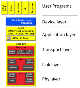
SATA is basically a point-to-point connection between a SATA host controller and a SATA device. As shown in Figure 1 multiple communication and processing layers are involved for full SATA functionality:
- Phy layer – which delivers the electrical interface and which nowadays can be fully implemented inside an FPGA.
- Link layer – sends and receives data frames and takes care of bit errors. In the SATA Host IP core this is built from programmable logic gates.
- Transport layer – controls the read and write operation via so-called Frame Information Structure (FIS) types and is also implemented from programmable logic gates.
- Application layer – handles standard ATA commands to the SATA device. An efficient implementation combines hardware and software.
- Device layer – serves as a hardware abstraction layer (HAL) to make SATA connected devices available to user programs.
- User program layer – comprises program suites for operating (and testing) SATA connected devices.
Modern FPGA devices feature so-called Multi-Gigabit Transceivers (MGT) which are suitable for many different high-speed serial protocols [4]. The SATA Host IP core from ASICS World Services utilizes these MGT to implement high quality SATA functionality, i. e. the Phy layer of the SATA Host IP core is completely done within the FPGA. There is no need for external Phy components.
The Link layer performs frame based transaction. It transmits and receives control primitives to manage the flow of frames. The Link layer creates a bridge between the Transport layer and the Phy layer. It encapsulates data frames in special symbols that indicate the beginning and end of a frame and removes those symbols on the receiving side. It also automatically asserts back pressure to the SATA device by inserting special hold primitives to throttle the transfers, and responds to back-pressure requests from the device by stripping hold primitives and waiting for valid data. Other responsibilities of the Link layer are to calculate and verify cyclic redundancy checks (CRC) and to scramble/descramble all transmitted data. Scrambling is an important part of the Link layer as it dramatically reduces Electro-Magnetic Interference (EMI).
Communication on the Transport layer is done via Frame Information Structures (FIS). The SATA standard defines this set of FIS types. Because this layer offers important performance trade-offs, we will have a more detailed look at the FIS flow between Host and Device for read and write operations.
As illustrated in Figure 2 the host informs the device about the current active operation via a Register FIS, which holds a standard ATA command. When the device is ready to transmit data it shall send one or more Data FIS and complete the transaction via a Register FIS Device to Host.
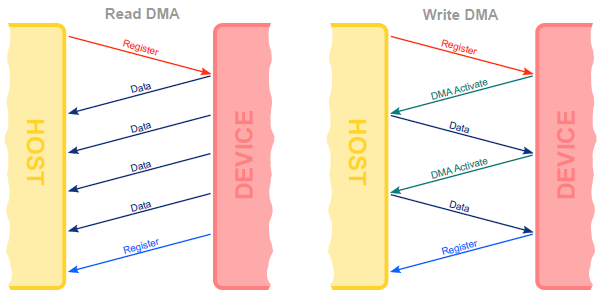
Figure 2 shows the FIS flow between host and device for a write DMA operation. Again the host informs the device of the operation via a Register FIS. When the device is ready to receive data it shall send a DMA Activate FIS and the host will start transmitting a single data FIS. When the device has processed this FIS and it still expects data it shall send a DMA Activate FIS again. In case of an error or a completed operation it shall complete the transaction via a Register FIS Device to Host.
A new feature introduced with SATA is the so-called “First Party DMA” (FPDMA). This transfers some control over the DMA engine to the device and thus enables the device for caching a list of commands and reordering these for optimized performance – so called “Native Command Queueing”. New ATA commands are used for First Party DMA transfers. As these commands are not necessarily instantaniously completed by the device, but rather queued, the FIS flow is a bit different for this mode of operation. The flow for a Read FPDMA Queued command is shown on the left hand side of Figure 3.
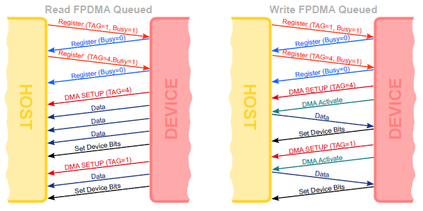
After receiving a Register FIS from the host the device queues the command and answers with a Register FIS to clear the busy field. Thus the host can send the next command. Each not yet completed command has a unique tag set to distinguish them. Each new command is added to the queue of the device and a scheduler in the device selects the command to be processed next. To process a command the device sends a DMA Setup FIS to the host with the tag field set accordingly. The DMA engine of the host then selects the scatterlist which belongs to the particular command and processes the data. To complete the transfer the device shall send a Set Device Bits FIS Device to Host.
As shown in Figure 3 the Write FPDMA Queued command is processed in a similar manner, but as in the non FPDMA mode again with a “ping-pong” of DMA Activate and Data FIS types. For efficiency the SATA protocol allows for an additional feature, the so-called “Auto Activation”, which will combine the first DMA Activate FIS into the DMA Setup FIS. Obviously this feature is only relevant for writes of smaller portions of data.
Communication on the Application layer uses ATA commands [2]. While a limited number of these commands certainly can be implemented as a finite state machine in FPGA hardware, a software implementation is much more efficient and flexible. Here, the Open Source Linux kernel provides a proven, standard implementation which almost exactly follows the ATA Standard and is proven in over a billion devices shipped.
The Linux ATA library, libATA, copes with more than 100 different ATA commands to communicate with ATA devices. These commands include not only data transfers but also provide functionality for S.M.A.R.T. (Self Monitoring Analysis and Reporting Technology) and for SECURITY features such as secure erase and device locking. The ability to utilize this code base, however, requires extra work of implementing hardware-dependent software in form of Linux device drivers as so-called Linux Kernel Modules.
GNU/Linux acts as a hardware abstraction layer between the user programs and the SATA Host IP core. Like in any other Linux based system, SATA devices are hidden behind a block layer which serves as a backend for the ATA library. All, read, write, or management operations can now perform on an abstract block device (/dev/sdX) without any special knowledge of the underlying SATA device itself. Even better, certain optimizations such as data caching and read-ahead transfers come with this software stack – fully integrated.
At this point the UNIX/Linux philosophy is reached which shields all devices via filesystems. Apart from “raw” data access one also can utilize the many different filesystems, for example, EXT2, EXT3, or XFS which GNU/Linux readily supports. These provide a robust and software developer friendly access.
When we say GNU/Linux we mean not just an operating system kernel but also the plethora of intgrated and pre-validated user space programs. Of particular interest are all tools for filesystem manipulation and for SATA device administration: Programs such as hdparm and smartctl give low-level access to SATA devices attached to the systems and can be used, for example, as a testbench or for performance analysis. This is complemented by full-featured Open Source test suites like bonnie++ and iometer.
Python scripting capablities and a C/C++ software development flow now make it very efficient to implement user programs and help focus on building the SATA-based application rather than spending valuable resources on SATA integration and debugging work. And, having a known-good environment also facilitates analysis during system architecture exploration.
Today, all these SATA layers can efficiently be implemented in Extensible Processing Platforms. However, when it comes to implementing a complete, reliable and high-performance SATA storage solution one must not ignore certain design space considerations:
First, only Phy, Link, and some portions of the Transport layer make sense to be implemented in programmable logic hardware and, thus, are provided when buying an IP core. Today, the decision whether to make or whether to buy a SATA host controller functionality is obvious: Buy an IP core. Very few design teams are capable to implement a functioning SATA host controller for the cost of licensing one.
Similarly, it makes little sense to spend significant time and money in-house to integrate this IP core into a programmable System-on-Chip, to develop device drivers for this core, and to implement application software for operating (and testing) this core. This is because the higher levels of the Transport layer, the Applications layer, the Device layer and the User Program layer are better to be implemented in software and, thus, typically are not part of an IP core delivery. This can create an unnecessary high burden of IP core integration and adds to the hidden costs of an IP core.
One of the reasons is that those higher layers depend on the target system’s architecture which again depends on the target system’s use case. Therefore, the second aspect often overlooked is that components such as Scatter-Gather DMA engines (which are hardware and software) must be implemented, tested and integrated to deliver a complete solution which ties together the IP core with the user programs.
Architectural Choices
In the following we will discuss design choices that allow you to scale the performance of a SATA storage implementation. The two fundamental metrics behind are:
- bandwidth and
- IO processing
Bandwidth is typically measured in MBytes/second, and especially for SSDs it makes sense to distinguish between bandwidth for reading data from the SSD drive, and bandwidth for writing data to the SSD drive. Today, most SSD drives reach the theoretical limit of 6 Gbits/second of the SATA-III link and deliver 500 MB/second read/write bandwidth, or more.
IO processing is measured in “IO Operations per second” (IOPS) for a defined blocksize of (typical) 4096 Bytes. Todays SATA SSD drives can support 80,000 IOPS for reads and 60,000 IOPS for write.
Reaching those performance values in an EPP-based programmable System-on-Chip is clearly possible, if one puts together the right micro-architecture of hardware and software components.
Both metrics, bandwidth and IOPS, significantly depend on the type of Direct Memory Access (DMA) and on the CPU’s ability to handle interrupts efficiently.
Importance of DMA Engines
With regards to DMA transfers, EPP can either use the built-in DMA engine, or a dedicated DMA engine, optimized towards the SATA IP core and implemented in the FPGA logic.
The EPP built-in DMA engine is an eight-channel PL330 DMA controller [1]. It is implemented as a hard IP core and, therefore, does not require any extra logic resources.
The built-in DMA engine does support Scatter-Gather mode, but unfortunately the current Xilinx Linux kernel driver lacks support for this functionality.
Even more, while being an eight-channel DMA controller it could even be used for NCQ. The only interface, however, to control the DMA engine is via an AXI slave interface. So you end up writing an AXI master IP Core anyhow, when you want to move control from software to custom logic.
Even with Scatter-Gather, there is another caveat when running an operating system (OS): How fast can the OS find new (large enough) free pages to sustain the data rate. This is mainly limited by the transfer size, the page size and the maximum number of segments the Scatter-Gather DMA engine supports.
When optimizing for SSD performance, the next bottleneck after resolving the scattered data bottleneck, are typically the IOPS. Once you can provide data fast enough for every single transfer, our experimental results below clearly demonstrate where the next performance bottleneck sits: Now the disc is sending “back-pressure” because of internal performance aspects due to the Flash memory access inside an SSD.
Good news: SATA has implemented a mechanism to counter that bottleneck, Native Command Queing (NCQ). Assuming you have multiple transfers to do, you can queue them up and the SSD selects the order of these accesses. To really gain performance out of this feature, it needs to be supported by the DMA engine. This is basically where DMA engine and Storage Controller IP-Core need to work hand in hand. The DMA engine knows about multiple transfers, each of them identified by a Tag, the SSD is notified about these transfers, reorders them and then requests them by sending a DMA Setup for the next Tag in the queue of the SSD. This is called Native Command Queueing. So both DMA Engine and Storage Controller need to know about the transfers, and thus need to be protocol specific for maximum performance.
For a low performance mass storage system the PL330 DMA-controller might be the quickest way to get an initial system up and running. Once this system needs more performance, one can either go for implementing the Scatter-Gather functionality or start using a custom DMA engine in the programmable logic. By the moment when the performance gain NCQ delivers is needed, one will, however, end up using a highly optimized DMA engine in the programmable logic. Today, the obvious design choice for SATA SSD performance is to integrate into the FPGA logic an NCQ-capable DMA engine optimized for SATA SSDs, such as the Performance DMA Engine from ASICS World Services, for exaple.
Aspects of CPU Interrupt Handling
Even with high performance Scatter-Gather DMA engine with NCQ support, implemented inside the FPGA logic, reaching the performance values of a modern SSD requires additional measures in the software domain. For data throughput with larger transfer sizes the optimizations done so far, will be sufficient. Once the transfer sizes become small (4096 Byte or even less), however, you will find, that the limiting factor will be the handling of interrupts generated by the storage controller.
Normally for every transfer, one interrupt is generated. So for 80,000 IOPS, this translates to 80,000 Interrupts per second. For a CPU running at 800 MHz, this gives you 10,000 instructions for saving the current state, switching into the interrupt context, completing the transfer (including error checking), restoring the state, and setting up the next transfer. The tough timing this causes can be relaxed a bit, by not using interrupts, but rather polling, to reduce the overhead caused by the switching and latency intruduced by the interrupt handling. When running the storage application as a standalone software, this is a lot simpler than when running inside the kernel of an operating system, such as an embedded Linux.
To reduce the stress put on such a system, it is better, to implement so-called Interrupt Coalescing (IC) functionality. IC works as follows: Instead of raising an interrupt everytime a transfer is completed, an interrupt is only generated every other transfer (and multiple tags are then flagged as completed). This can be implemented inside the FPGA logic, by having a completion register bit per tag, a counter for counting the number of completions, and a timer, for generating a timeout (such that single transfers get completed as well).
Experimental Data
Based on the observations from the previous section and measurements on comparable plaforms, we can expect the following qualitative results. 1 For a simple DMA engine, implemented inside the programmable logic or in terms of the PL330 with the standard driver, we will see low data throughput, with increasing values when plotted over the transfer size. There are basically two limiting factors here: for small transfer sizes the interrupt handling and DMA setup latencies will are the limiting factor and when running under an operating system, another limiting factor will be caused by the lack of larger consecutive blocks of memory available from the memory management to satisfy the simple DMA data transfers.
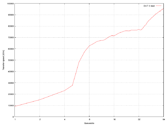
Figure 4 to 7 show an examplary plot of read and write speeds for 4096 Byte transfers over various NCQ-table lengths. In this case a “Simple DMA Engine”, described above, is comparable to an NCQ-table length of 1.
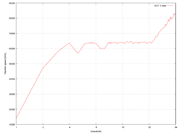
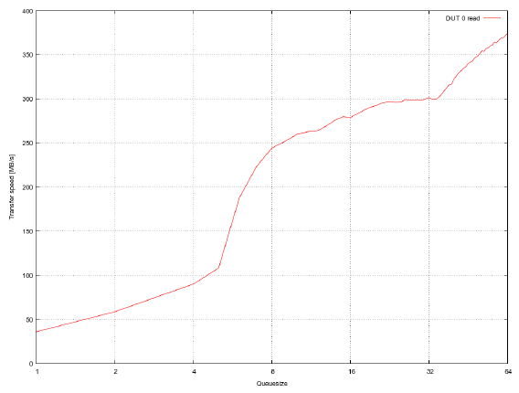
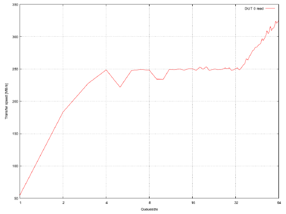
To overcome the memory management bottleneck an OS introduces Scatter-Gather functionality in the DMA engine can ensure that even for large transfer sizes one setup for the DMA engine is sufficient. This way no degradation in the performance for large transfer sizes can be observed. For large transfers the setup time of the DMA engine and the completion time of a transfer shows less effect, thus allowing for high bandwidth throughput of data.
To eliminate the remaining setup latencies and wait states hardware support for FPDMA inside the DMA engine allows for even better performance, by significantly increasing the IOPS, as shown in the example in Figures 4 to 7 The data in these plots were captured on a high end workstation to eliminate the bottleneck introduced by the interrupt load, which can later be reduced by introducing interrupt coalescing.
Reference
[1] Zynq-7000 All Programmable SoC, Technical Reference Manual. Tech. rep., Xilinx, Inc., November 2012. Visited on January 18th, 2013.
[2] INTERNATIONAL COMMITTEE FOR INFORMATION TECHNOLOGY STANDARDS. AT Attachment 8 – ATA/ATAPI Command Set, September 2008. http://www.t13.org/.
[3] THE SERIAL ATA INTERNATIONAL ORGANIZATION. Serial ata international organization.
http://www.sata-io.org.
[4] XILINX, INC. Virtex-5 FPGA RocketIO GTX Transceiver User Guide, October 2009.
http://www.xilinx.com/bvdocs/userguides/ug198.pdf.
🌐 www.missinglinkelectronics.com
MLE (Missing Link Electronics) is offering technologies and solutions for Domain-Specific Architectures, which focus on heterogeneous computing using FPGAs. MLE is headquartered in Silicon Valley with offices in Neu-Ulm and Berlin, Germany.