Deep Image Analysis for Multimedia Systems
Debugging a video image system, especially if multiple displays are involved, can be a very hard task. Pixel-accurate and color-correct snapshots, triggered by external events and precisely timestamped can greatly aid the process. If additional real-time preprocessing of the video image stream can be accomplished, certain testing scenarios can profit even further. Utilizing the “Soft” Hardware of the MLE 1000 Series Rapid Prototyping System, a framework for simultaneous Deep Image Analysis of multiple displays is demonstrated.
Copyright © 2026 Missing Link Electronics. All rights reserved. Missing Link Electronics, the stylized Missing Link Electronics MLE logo are the service mark and/or trademark of Missing Link Electronics, Inc. All other product or service names and trademarks are the property of their respective owners.
With many modern infotainment and multimedia systems controlling more than one display, new software and system verification challenges arise. It is now necessary to have a look at all connected displays at the same time to perform complete system validation. It is not sufficient to have access to the meta-information like text output that the software intends to display on the screen, but the real image on the screen has to be monitored. This may also include Deep Image Analysis using image processing and/or optical character recognition (OCR) technology. Additionally, timing analysis is crucial to gain knowledge of the system behavior. For example, the reaction time from stimulus (e.g. a button press or messages on communication interfaces) to display change (e.g. a new screen image) may have to be measured as well as the synchronicity if multiple displays are involved. While this validation itself is a demanding task, debugging a perceived problem is even harder. Exact timing information of events happening before the failure is needed to distinguish the cause from the symptoms.
Challenges when building a test and debug environment include adapting to the vast diversity of displays and their connection standards as well as handling the huge bandwidth which multiple video image streams may produce.
In the following we will describe possible debugging aproaches for multiple video image display systems, followed by an explanation of two commonly used video image transmission standards. Having introduced the basic standards, we will describe in detail a Deep Image Analysis Framework based on the MLE 1000 Series Rapid Prototyping System, which can be used to solve the problems outlined above.
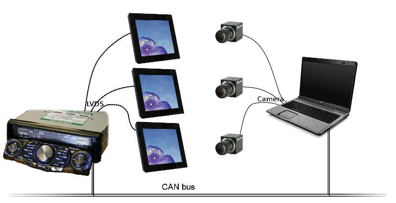
To obtain access to the displayed image data on the screens, different possibilities exist. One is to install cameras in front of the displays and capture their content (Figure 1).
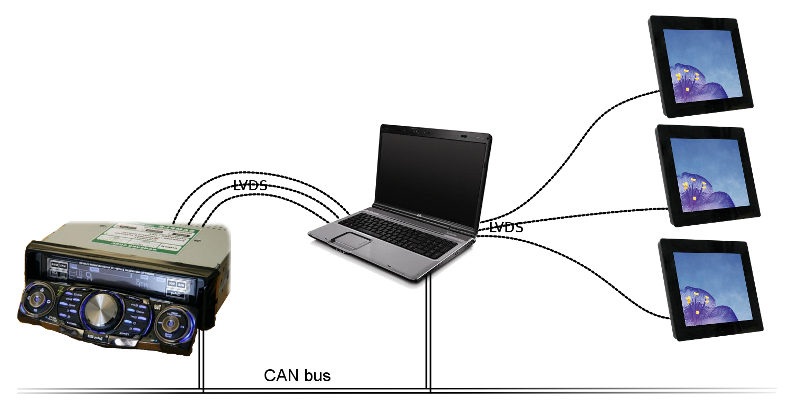
The second one, a more direct approach, is to replace the displays with a device acting as a spy as if it were a display, but actually being able to capture the images. As an option, this device could simultaneously forward the image data to the one or more target displays.
The latter method, from now on called Deep Image Analysis, eliminates some drawbacks of the camera approach. It is independent of the physical setup of the components and so no keystoning effects have to be corrected by precisely adjusting camera angels or using software post-processing. Also, all other types of image distortions caused by the lens of a camera, like barrel or pincushion distortions and chromatic aberration, are eliminated. The Deep Image Analysis Framework presented here is pixel accurate and color correct by design, which simplifies image analysis for system debug or even OCR. Furthermore, this approach is frame accurate and makes precise timing measurements possible.
There are on the other hand some demanding challenges to accept. As normal Personal Computers (PC) cannot directly connect to thin-film transistor (TFT) displays or their respective video image sources special hardware in the form of a so called framegrabber add-on cards has to be added. Also, video image processing quickly requires a high performance PC as soon as multiple streams should be handled. For example, at 800 x 480 pixel per frame resolution and a color depth of three bytes per pixel, a 60 frames per second video image stream results in a bandwidth of about 70 MByte/s per display. Besides, the number of slots for add-on cards available in the PC is limited and this limits the number of displays that can be connected. Figure 2 shows such a setup, where video image processing on the Central Processing Unit (CPU) may become a bottleneck.
As will be shown, a Deep Image Analysis Framework utilizing an MLE 1000 Series Rapid Prototyping System is easier to build and more cost efficient than a solution solely based on PC technology. This way the data streams and pre-processing are kept outside the PC (Figure 3) which considerably offloads the PC from heavy computing. An entry level MLE Rapid Prototyping System already offers 16 freely configurable low-voltage differential signaling (LVDS) lanes (LVDS is a common electrical interface for displays). This is sufficient for simultaneously handling two display inputs and two corresponding display outputs of the 18 bpp display type (see below). Multiple LVDS-based logical interface and protocol standards exist to which the Field Programmable Gate Array (FPGA) based MLE 1000 Series Rapid Prototyping System can be adapted. For an example of LVDS connectivity consider the MLE TechBrief on connecting multiple LVDS cameras to such a system [TB20091127]. The large bandwidth and processing requirements multiple displays impose are easily handled by the parallel hardware inside the FPGA.
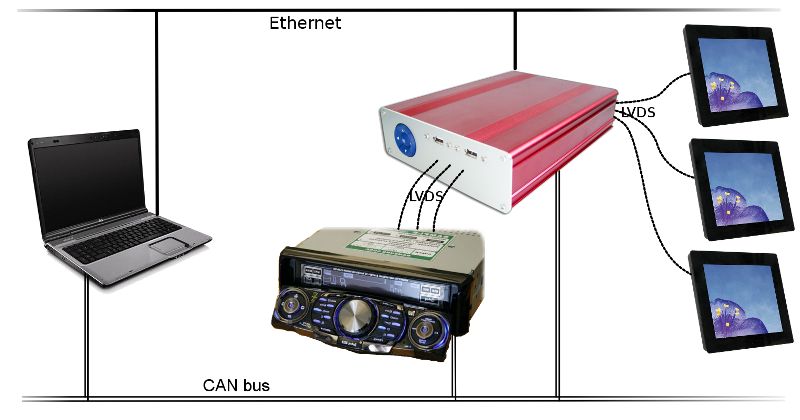
Also MLE has a full featured Linux operating system, which offers easy access to the captured images, as well as a broad range of connectivity options to store or transfer the obtained data. These interfaces include Universal Serial Bus (USB) to store images, and Ethernet and Controler Area Network (CAN) to connect to the analysis system as well as the rest of a potential testing environment.
For triggering a snapshot multiple options are available. Possible trigger conditions are Ethernet packets, signals on General Purpose Input/Output (GPIO) lines, certain criteria of the image itself or CAN messages, which is of special interest for automotive testing environments. As this happens directly in the parallel FPGA logic, the reaction time is extremly short and typically faster than 1 µs.
Before describing how to build a Deep Image Analysis Framework on top of a MLE 1000 Series Rapid Prototyping System, we will have a detailed look at TFT display interface standards. Therefore we first explain the parallel data format of the video image signal used inside the video image source, the FPGA and the display. Then we will show how this data translates to the LVDS links, used for video image transfer between devices. The interested reader can find further details in the LVDS Video Interface reference design [RD1030] by Lattice Semiconductor and the application note on LVDS fundamentals [AN-5017] by Fairchild Semiconductor.
The parallel video image data transmission lines and their timing can be seen in Figure 4.
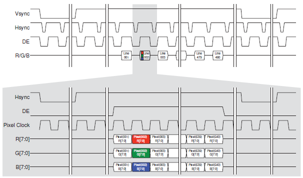
All lines are single-ended, i.e. the voltage level on each single wire defines whether this line represents a digital one or zero. The color of each pixel is composed of the three basic colors red, green and blue; the intensity of each of this colors is usually given by a 6 bit or 8 bit value per color. Because there is no fixed frequency for the transmission an additional signal line, the pixel clock, is used to mark the transition from one pixel to the next.
By convention this continuous stream fills each line of the frame, which is a single image in the video image transmission, with pixels from left to right and the frame itself with lines from top to bottom. To be able to detect the beginning and length of these lines, an additional signal, called horizontal synchronization or hsync signal, is needed. It’s rising edge marks the transmission of the first, i.e. leftmost, pixel in a line and it’s falling edge ends the line. Due to historic reasons not the complete line is visible, because cathode ray tube (CRT) monitors needed a pause in the transmission to move the electron beam from the end of one line to the beginning of the next. So in digital video image transmissions an additional data_enable signal is used, marking exactly the visible part of each line.
The one piece of information still missing to successfully display the video image stream is, which line is the first in each frame. So analogous to what the hsync signal does for lines, the rising edge of the vertical synchronisation signal vsync marks the first line of the frame and the falling edge ends the frame, thus defines it’s height. Here again, more lines are transmitted than are actually visible, because old CRT displays needed a pause to move the electron beam from the last line to the first line of the new frame. In contrast to the pixel data for lines, visible lines are not marked by a dedicated data valid signal. They can be detected and ignored by monitoring the pixels data_enable line. If this line is inactive for the complete length of the line, the line contains no data to be displayed.
Today, the above described scheme with it’s many parallel single-ended signals is more and more left to internal video image processing in devices. For inter-device connectivity LVDS transmission, high-speed differential signaling is now widely used. LVDS uses two corresponding wires, with the voltage difference between both wires defining the state of the according data bit, high or low. Because these two wires shall be placed physically close to each other, noise affects both of them in the same way, maintaining their voltage difference and thus the value of the bit.
This makes the transmission more robust against electromagnetic interference (EMI) and allows for lower signaling voltages and higher transfer speed compared to single-ended transmissions. As LVDS lines can be used at much higher frequencies, it is possible to transport the same amount of data over fewer wires compared to the above described parallel case.
This is done by serializing the data, i.e. multiple bits that once were present at the same point in time on multiple parallel wires are now transmitted one after the other on a single line. A common constellation for displays with a color depth of 18 or 24 bits per pixel is using three or four LVDS pairs, respectively. This is done by serializing 21 parallel lines (18 color lines as well as one hsync, one vsync and one data_enable line) into three LVDS lanes, or, in case of higher color depth, serializing 27 parallel lines (24 color lines as well as one hsync, one vsync and one data_enable line) plus one unused dummy bit) into four LVDS lanes. So as the number of wires is reduced by a ratio of seven the clock frequency has to be raised by this ratio of seven to maintain the overall data throughput and thus framerate.
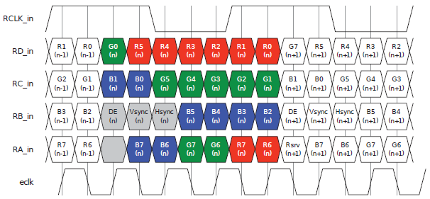
In either case, this results in seven bits per LVDS lane being transmitted during one cycle of the original pixel clock. Figure 5 shows a common mapping of parallel signal lines to LVDS bits.
Depending on the pixel protocol used, this mapping may vary, but can easily be dealt with inside the configurable FPGA, as we will demonstrate later. The pixel clock, transferred over an additional dedicated LVDS pair, remains at it’s original frequency, and thus also acts as a framing signal for the data bits of each pixel. For the actual implementation it is noteworthy that the protocol adds a two bit offset between the pixel clock and the beginning of this pixel’s data.
In our Deep Image Analysis Framework we receive LVDS video image input from multiple TFT data sources, process it, and then again generate LVDS video image output. For simplicity, in our example setup all LVDS links described have one clock and three data lanes. However all aspects also apply to the case of one clock and four data lanes for the transmission. For the processing we need de-serialized parallel video image data, because of both, the lower, easier to handle, frequencies, and the fact that the complete color information for a pixel shall be available at a single point in time. So one step (see below), will be to convert from LVDS signals to parallel video image data and back.
The following describes a Deep Image Analysis Framework based on an MLE 1000 Series Rapid Prototyping System in a top-down fashion.
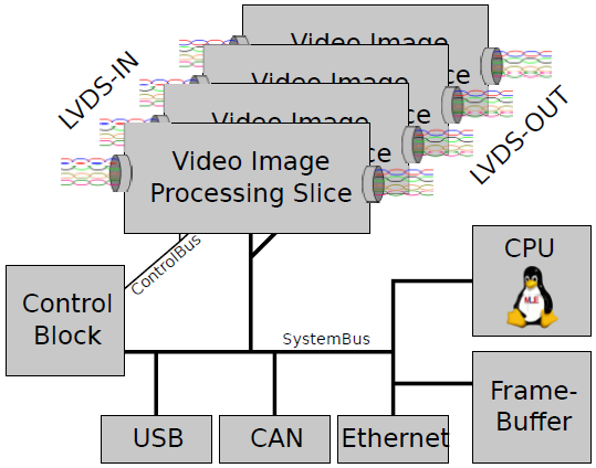
The whole architecture, as seen in Figure 6, is based on a PowerPC processor (CPU) running Linux and having peripherals attached to a system bus. These are, among others, the communication interfaces for USB, Ethernet and CAN. The video image data is processed in dedicated Video Image Processing Slices, each capable of handling one LVDS display input and one output. To support more displays, multiple Video Image Processing Slices can be added to the system. Each of the Video Image Processing Slices is connected to the system bus to be able to transfer snapshots or complete video image streams to the Framebuffer. Operation is controlled by a separate Control Clock, in charge of handling and forwarding trigger events as well as generating timestamps. The Control Block itself can be accessed from Linux via it’s system bus attachment for configuration.
In Figure 7, an example Video Image Processing Slice for a 18 bit per pixel display, using a total of four LVDS lanes, is shown. Other standards can be integrated in a similar way, using different input and output blocks. These blocks, the deserializer SerDes_IN for converting a serial LVDS stream to parallel video image data and the serializer SerDes_OUT converting parallel data back to LVDS, are located at the beginning and end of the processing chain.
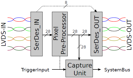
Once the stream is converted to the parallel pixel format, a hardware Pixel Pre-Processor can apply pixel based algorithms to the frames and can optionally analyze the data to drive a trigger output if certain criteria match. The filtered video image stream is then forwarded to the output block and a Capture Unit, which will transfer the frame visible at the time the trigger condition is met to the Framebuffer. As a special option one can select whether the video image stream shall be displayed after being processed, in which case the Deep Image Analysis Framework acts in a Man-in-the-Middle-Mode and the pre-processed result becomes visible, or wether the original frames are displayed, working in so-called Spy-Mode. Figure 7 shows the Man-in-the-Middle-Mode, but also hints Spy-Mode, where input and output blocks are directly connected. In Spy-Mode the output block will ignore the parallel video image data input.
Processing the video image data in parallel inside reconfigurable FPGA hardware is extremely fast and more efficient compared to a general purpose CPU implementation in software. In general, bitlevel parallel compute tasks run much more efficient in a parallel FPGA fabric than on a sequential CPU , an aspect which is explained, for example, in the MLE article [Santak2010] about Advanced Encryption Standard (AES) cryptography.
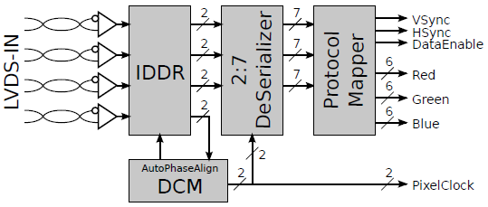
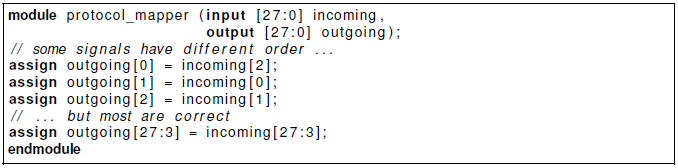
The process of generating the parallel data takes place in the deserialization unit SerDes_IN shown in Figure 8, directly followed by a protocol specific Protocol Mapper, that ensures the correct order of the signal lines.
Ordering is necessary because different implementations of the video image data transfer protocol exist even at this level. Although the electrical interface and the transfer type are identical, the mapping of parallel video image data lines to LVDS bits may be different. Similar to a hardware crossbar, the Protocol Mapper does exactly such a protocol-specific adaption. From the Verilog HDL code shown in Listing 1 it is obvious how easy and efficient such computations can be implemented in FPGA technology, while it would be very compute intensive to do the same on a CPU.
As the MLE 1000 Series Rapid Prototyping System’s uses a Xilinx Virtex-4 FPGA, the dedicated ISERDES and OSERDES blocks this family offers, could be used for (de-)serialization, as described in the Xilinx application note for LVDS transceivers [XAPP704]. Unfortunately, this particular video image application requires a higher clock frequency than supported even by the fastest Xilinx Virtex-4 FX device, because the Digital Clock Manager (DCM) integrated in this FPGA has to generate a sample clock at a ratio seven times higher than the input pixel clock (see LVDS paragraph).
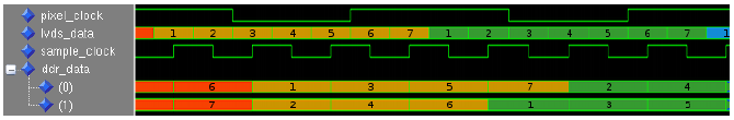
The frequencies used for this video image transmission (the example display has a resolution of 800 x 480 pixels and a framerate of 60 Hz; taking the additional time for non visible parts of the transmission into account, this leads to a 33 MHz pixel clock) will force us to use the DCM’s lowspeed mode, in which the resulting 231 MHz output clock would be above the allowed maximum output frequency of the DCM – see Xilinx’s [DS302]). A solution to this would be to use the Double Data Rate (DDR) mode ISERDES also offers, allowing the sample clock to be half the speed, and thus in the valid range, but then the de-serialization ratio of seven is not possible. Fortunately, one can also implement the deserialization entirely inside the FPGA’s configurable fabric. We can use the IDDR and ODDR blocks of the Xilinx Virtex-4 to split each LVDS lane, operating at 231 Mbps, into two signals, carrying data each at 115.5 Mbps. Figure 9 shows the input lvds_data to an IDDR block, the pixel_clock, the sample_clock and the resulting two output ddr_data signals after the DDR sampling.
Each set of bits belonging to one pixel is marked with a different color and the bits composing a single pixel are numbered, to give a better understanding. The most outstanding characteristic of a DDR transmission is that data is sampled on rising AND falling edge of the sample_clock. The IDDR block sends lvds_data sampled on the rising edge of the sample_clock to it’s first output ddr_data(0), data sampled on the falling edge to the second, ddr_data(1). Combined with the uneven multiplication factor of seven between pixel and sample clock, this leads to alternating positions of the bits of each pixel on the two outputs, which has to be taken into account when re-assembling them later.
The remaining task now is to build a deserializer that translates these two lines which operate at lower clock frequencies into seven signals per LVDS lane representing the seven bits transfered during one clock cycle. This involves using shift registers, to fetch the data, and parallel registers, to store the output, as well as a state machine taking care of the mentioned fact, that bits have alternating positions on the signal lines.
The IDDR block needs a clock signal matching the incoming data rate, with edges in the center of the data eye, to achieve the best possible sampling result. But as the sample clock is generated by a DCM it is in phase with the original pixel clock, thus the edges of the sample clock match with the edges of the data bits. What is needed to achieve a correct data sampling is a phaseshift of the sample clock. This can be done using the “fixed phaseshift” feature of the Xilinx Virtex-4 FX DCM using pre-calculated values or by an Auto Phase Align unit, which searches for the optimal sampling point everytime a new video image source is connected. As a known pattern for this search, the input pixel clock can be used and compared against.
In the Deep Image Analysis Framework the triggering of a snapshot is done by a Control Block that can use multiple sources for it’s trigger decision. These can be the output of the mentioned Pixel Pre-Processor or the Linux system monitoring GPIOs, Ethernet and CAN or other interfaces you need. The design of this unit is left to the imagination of the test engineer and will probably be a custom state machine matching the requirements of a particular application. Obviously, the Control Block can furthermore be used for additional functionality, for example, to timestamp the snapshots.
The MLE 1000 Series Rapid Prototyping System has a full featured Linux system running on the embedded PowerPC processor. This can be used to control all further processing of the captured frames. The frames were stored in the Framebuffer memory by the capture hardware and are therefore accessible to Linux via the standard framebuffer device driver. For example, the Open Source fbgrab application [FBGrab], pre-installed on the MLE 1000 Series Rapid Prototyping Systems, can be used to store the captured frames as standard image files, for example in the Portable Network Graphics (PNG) format. A Linux application may then decide to apply further processing, may it be in software or utilizing the FPGA’s huge parallel compute power. Additionally the images can be stored onto a USB-Stick or transferred over Ethernet to a testsystem, typically a PC at a test engineer’s desk, for further analysis and inspection.
In this paper we have shown, that MLE’s approach of “Soft” Hardware with it’s programmable IO connectivity and parallel processing power, enables an efficient implementation of a Deep Image Analysis Framework. This can, for example, be used for the validation of infotainment systems with multiple displays, where it delivers pixel accurate, precisely timed and pre-processed information to the analysis software thus easing the use and implementation of the later.
Because of the many I/O connectivity options of the MLE 1000 Series Rapid Prototyping System various trigger sources are possible to initiate a snapshot of a video image stream. These sources can for example be certain criteria of the images itself, Ethernet or CAN messages, GPIO signals or a software script as well as human input. Captured frames can then be stored on an attached USB-Stick or transfered to a PC for further analysis using standard network connectivity and protocols.
References
[TB20091127] Missing Link Electronics:
LVDS Connectivity for the MLE 1000 Series, November 2009.
http://www.missinglinkelectronics.com/MLE-TB20091127
[Santak2010] Leo Santak, Dr. Endric Schubert:
AES-Beschleunigung über Befehlssatzerweiterung: Die eigene Crypto-Engine im Xilinx-FPGA, Elektronik embedded, WEKA FACHMEDIEN GmbH, February 2010.
[UG70] Xilinx, Inc.:
Virtex-4 FPGA User Guide, December 2008.
http://www.xilinx.com/bvdocs/userguides/ug070.pdf
[DS302] Xilinx, Inc.:
Virtex-4 FPGA Data Sheet: DC and Switching Characteristics, September 2009.
http://www.xilinx.com/support/documentation/data_sheets/ds302.pdf
[XAPP704] Xilinx, Inc.:
Virtex-4 High-Speed Single Data Rate LVDS Transceiver, February 2005.
http://china.xilinx.com/support/documentation/application_notes/xapp704.pdf
[AN-5017] Fairchild Semiconductor, Inc.:
Application Note: LVDS Fundamentals, December 2000.
http://www.fairchildsemi.com/an/AN/AN-5017.pdf
[RD1030] Lattice Semiconductor, Corp.:
Reference Design: 7:1 LVDS Video Interface, September 2009.
http://www.latticesemi.com/dynamic/view_document.cfm?document_id=21823
[FBGrab] FBGrab website.
http://hem.bredband.net/gmogmo/fbgrab/
🌐 www.missinglinkelectronics.com
MLE (Missing Link Electronics) is offering technologies and solutions for Domain-Specific Architectures, which focus on heterogeneous computing using FPGAs. MLE is headquartered in Silicon Valley with offices in Neu-Ulm and Berlin, Germany.