NVMe Streamer for High-Speed FPGA Data Acquisition & Recording
This Technical Brief is about FPGA high speed data streaming, explaining how to best record data that is received by an FPGA, for example from high-speed data acquisition, and that needs to be stored into an NVMe SSD (Non-Volatile Memory Express Solid-State Drive), after FPGA-based Data-in-Motion processing; or the opposite direction when data streams out of an SSD into an FPGA for Data-in-Motion processing.
Copyright © 2026 Missing Link Electronics. All rights reserved. Missing Link Electronics, the stylized Missing Link Electronics MLE logo are the service mark and/or trademark of Missing Link Electronics, Inc. All other product or service names and trademarks are the property of their respective owners.
At MLE we have been using PCIe and NVMe for FPGA-based systems for a while, mostly to implement so-called Domain-Specific Architectures for high-performance systems (embedded, or not). In this document we will show architecture choices for CPU-less NVMe SSD reading/writing, for example for streaming applications where data-in-motion gets processed by FPGA fabric and then needs to be recorded.
Example FPGA high speed data streaming applications are active / passive MIMO Radar, 10/25/50/100G networking, hyper-converged storage servers, Automotive Advanced Driver Assist Systems (ADAS), Autonomous Vehicle sensor recording, etc. We refer to this NVMe data streaming IP core for high speed data acquisition as “NVMe Streamer”.
1. Motivation and Outline
Modern FPGA fabric not only allows Data-in-Motion processing at Terabits-per-second speeds but also has high-speed serial IOs to implement PCI Express (PCIe) Standards 3.0 or 4.0, or newer. Non-Volatile Memory Express (NVMe) is a fairly recent storage protocol that sits on top of PCIe and reduces the software processing burden compared to legacy AHCI protocol used for SATA. A wide range of different SSD form factors are available today, for example NGFF m.2 or U.2 or new Enterprise and Datacenter SSD Form Factor EDSFF E1.S or E1.L. The combination of both, FPGAs and NVMe SSD, allows to implement high-speed data acquisition systems, a.k.a. data recorders or data loggers.
Fig. 1 shows an FPGA-based architecture where ingress data is to be recorded using an NVMe SSD and where this NVMe SSD is connected to the Programmable Logic (PL) using High-Speed Serial IO for PCIe. Basically, incoming data enters the PL on the left, suitable for data-in-motion processing of that data inside the FPGA, before this data gets written into the NVMe SSD.
The commonly used data flow is also shown in Fig. 1. The NVMe protocol is handled in software by an Operating System – typically Linux – which runs on the Processing System (PS) a.k.a. the CPU. The NVMe and PCIe software routines use Direct Memory Access (DMA) to write the data from Main Memory into the NVMe SSD and, therefore, there is a previous DMA required to transfer the data from the PL into Main Memory.
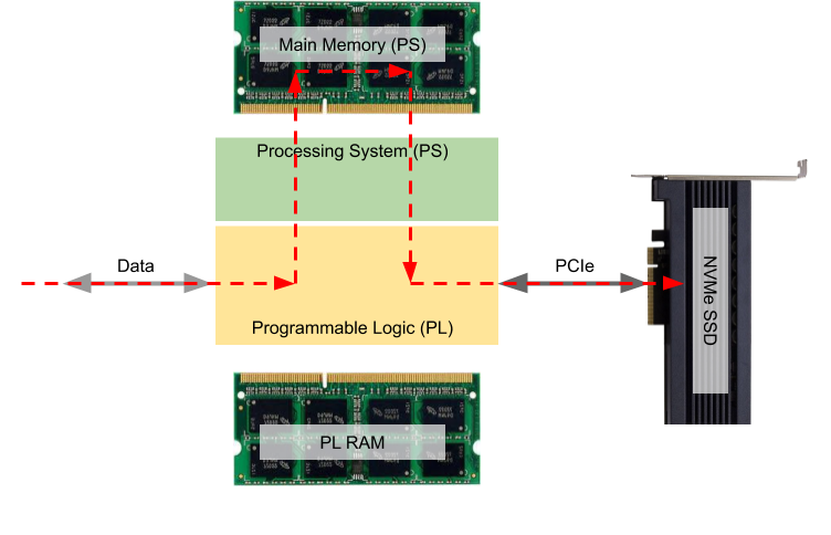
Obviously, in Fig. 1 the data takes a “detour” and this adds traffic to the memory bus of the PS which in a typical system likely becomes the system’s performance bottleneck.
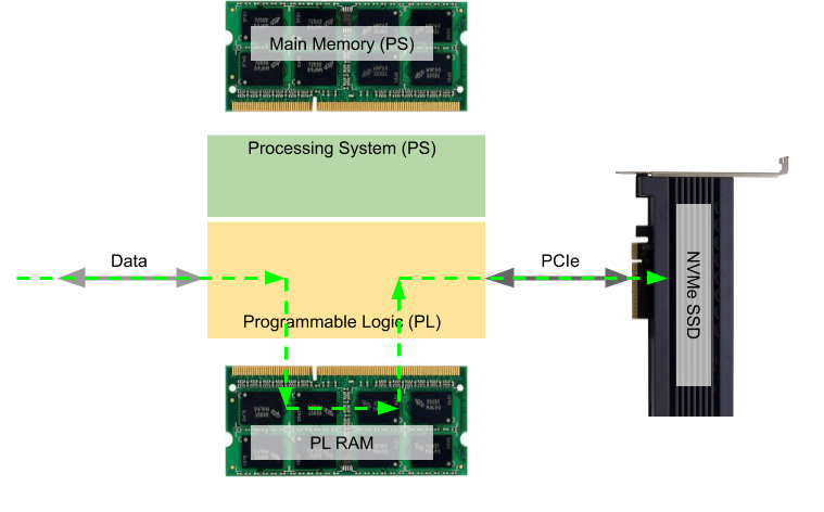
The objective of our FPGA IP core for high speed data acquisition, NVMe Streamer, is to free up the Processing System, regardless of whether this is an embedded CPU like the ARM A53 in the Xilinx Zynq Ultrascale+ MPSoC, or a companion CPU attached to Programmable Logic. This is shown in Fig. 2: The dataflow can stay entirely within the Programmable Logic and, optionally, be buffered using PL-attached RAM. Such a buffer may be needed because most SSDs, while supporting sustained writing at high bandwidth over extended periods of time, may take short “pauses” in the range of milli-seconds. Even if those pauses happen rarely, this may become a problem if the data source does not support backpressure; without any buffering data may get lost. As we will discuss below, the size of such a buffer can be between 512 kB – which fits on-chip RAM (URAM) – and up to Gigabytes, if needed.
Over the following pages we will explain the basic functioning of NVMe, as it is necessary to understand how our NVMe Streamer architecture works, and how it can best be utilized. Then we go into the details of our NVMe Streamer and close by sharing some experimental data with you.
2. Non Volatile Memory Express (NVMe)
To better understand the functioning of our FPGA IP for high speed data acquisition, NVMe Streamer, we need to dig a little bit into the basics of the NVMe protocol. For more info about NVMe and in particular the NVMe specification (currently published as Revision 1.4) we recommend you visit the NVMe Website.
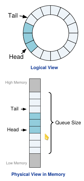
Key to NVMe is its concept of NVMe Queues which are implemented as circular buffers. NVMe distinguishes between two types of queues: I/O Queues used for I/O Commands (which is “reading” and “writing” data) and Admin Queues for the administration commands – used to configure those I/O Queues and for controller management. Each type has a so-called Submission Queue (SQ) used from the host to the device to send commands, and, typically, for each SQ a corresponding Completion Queue (CQ) from the device back to the host to post command completions. All those commands and completions are transported by PCIe Transaction Layer Packets (TLP). The NVMe specification allows for up to 64K I/O SQs and CQs and each queue can have up to 64K entries. This makes very scalable systems where one or more queues can run – as software – on a CPU Core (to be precise, each CPU Core can work on its own set of queues with no inter-core locking or communication required; this is very different from for example AHCI with just one queue).
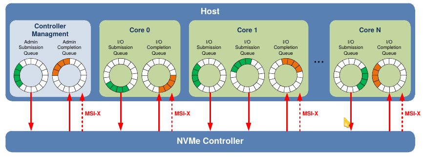
For the NVMe Streamer we have implemented I/O Queue handling in Programmable Logic. This gives us deterministic timing behaviour and allows to scale performance (read/write bandwidth) along with the attached NVMe SSD. Admin Queues which are not in the data path for reading/writing and thus have no impact on performance we run as bare-metal software in a small embedded CPU.
Btw, if you want to know more about NVMe, here is a nice tutorial given by Kevin Marks at the Flash Memory Summit 2013.
3. NVMe Streamer Architecture – High Speed FPGA Data Acquisition
First, our FPGA IP for high speed data acquisition, NVMe Streamer, is implemented entirely in Programmable Logic. This allows you to implement a high-speed data acquisition system even when using an FPGA without integrated CPUs, such as Xilinx Kintex or Virtex Ultrascale+ FPGAs, for example.
Second, for resource efficiency and to scale read/write performance along with the NVMe SSD, we use parameterizable AXI4-Streams, as shown in Fig. 3:
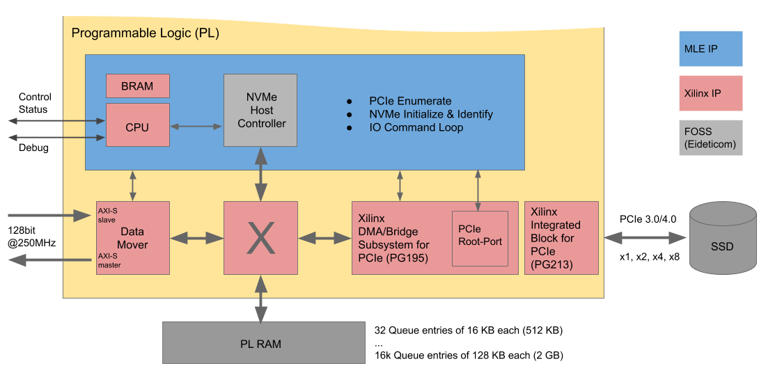
Today, most NVMe SSDs have a PCIe 3.0 x4 connection which has a theoretical bandwidth of 4GB/s. Thus the data input and data output of our NVMe Streamer each are implemented using 128 bit wide AXI4-Streams running at 250 MHz. These feed into an memory-mapped AXI4-Switch, connected to an NVMe Host Controller, to (optional) PL RAM, and to the DMA/Bridge Subsystem for PCIe. This DMA/Bridge PCIe Subsystem has a block which is configured to be a PCIe Root-Port and ultimately connects to the NVMe SSD via one of the PCIe Hard-IP Cores.
This datapath is controlled by a combination of a Xilinx MicroBlaze embedded CPU and an Open-Source NVMe Host Controller which is responsible for issuing NVMe requests and receiving NVMe responses. The CPU runs a bare-metal software for NVMe Admin: Upon start-up this software does the so-called PCIe Enumeration and, thereby, “finds” the attached NVMe SSD. Although our block diagram only shows one NVMe SSD, in principle multiple SSDs can be attached, depending on your storage capacity needs. The NVMe SSD is initialized and identified (using the NVMe “identify” namespace command). Once everything has been set up, this software switches over to I/O Queue handling, effectively for reading/writing data from/to the NVMe SSD.
The footprint of this software is small and thus, we only need a little BRAM. This software also manages an AXI4-Lite interface for control and status plus a debug UART. The control and status commands you can issue via this interface are:
- Get media size and model information of attached SSD
- Set starting write address on SSD medium
- Set maximum write address on SSD medium
- Start and stop writing
- Set starting read address on SSD medium
- Set maximum read address on SSD medium
- Start and stop reading
3.1 Buffers for Gapless and Lossless Recording with SSD
A word on the (optional) PL-RAM: Depending on your application and the specs of your NVMe SSD you may or may not need this RAM as a stream buffer!
Modern SSDs support sustained writes at high data rates. However, every now and then the SSD may take a small “pause” of a few milli-seconds from writing, for internal house-keeping etc. If your data source does not support back-pressure, like a camera, for example, then you will need to buffer the data to avoid data loss.
To better understand this SSD behavior, we have included some charts from www.storagereview.com and from www.tomshardware.com .
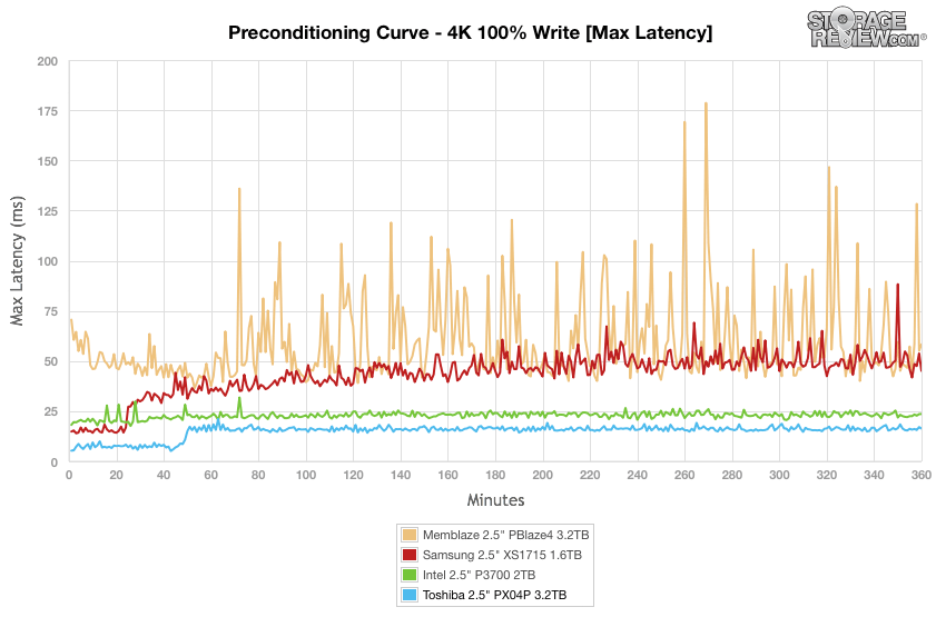
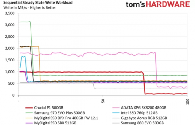
As Fig. 4 shows, many SSDs reduce bandwidth performance when writing data over long periods of time. This is due to the Flash Translation Layer (and sometimes also to protect the SSD from overheating) and, obviously, depends on the Flash Controller integrated, what type NAND Flash has been used, SLC, MLC, TLC, QLC, etc. and other SSD details. The article “Your Next SSD Might Be Slower (Thanks to QLC Flash)” elaborates on that topic.
From our experience at MLE, this behaviour can even be different for SSDs from the same vendor, same model but different capacity or firmware. That’s why we recommend to always consult your SSD vendor’s datasheet!
But, what are the implications when building a gapless recording application? When do I need buffers, and at what size?
If your data producer supports back-pressure, obviously, you won’t need any stream buffer. But, if you are using cameras or similar sensors which can not be stalled, you will need a buffer, for those short moments when the SSD cannot digest any data. Therefore, our AXI4-Switch streams the data through a stream-buffer to avoid data loss (i.e. recording “gaps”). This is parameterizable by you as follows:
- You can select the length of the I/O Queues. A reasonable minimum number would be 32 Queue Entries which still gives you OK performance. A sensical high value would be 16k Queue Entries.
- You can also pick a size for the Queue Entries, starting from a reasonable low value of 16k Bytes up to, for example, 128k Bytes. Typically you want to adjust the Queue Entry size to match the granularity of the data you want to record as well as the NVMe SSD’s spec.
For a minimum buffer you will only need 512k Bytes (32 * 16 kB) which fits well into the UltraRAM of many FPGA devices. A large buffer may be up to 2 GB (16k * 128 kB) which can be external DDR RAM, or integrated HBM2 RAM.
3.2 IP-Core Landscape of MLE NVMe Streamer for High Speed FPGA Data Acquisition
For cost and maintenance reasons we have integrated 3rd party IP Cores from Xilinx and from the Open-Source Community to implement NVMe Streamer. The most important Xilinx IP Cores are all free-of-charge and come with the Xilinx Vivado tool:
- PG085 – AXI4-Stream Infrastructure IP Suite v3.0 for Vivado Design Suite
- PG059 – AXI Interconnect v2.1 for Vivado Design Suite
- UG984 – MicroBlaze Processor v11.0
- PG194 – DMA/Bridge Subsystem for PCI Express v4.1
- PG213 – UltraScale+ Devices Integrated Block for PCI Express v1.3
The Open-Source IP Core originates from our fellow Xilinx Alliance Partner Eideticom and initially was implemented as an NVMe Host Controller for IBM’s OpenCAPI / SNAP.
3.3 Applications & Use
The following Fig. 5 shows an exemplary hardware test setup based which we have been using at MLE for development and lab testing purposes.
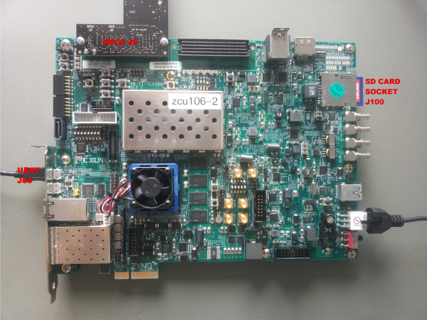
Hardware includes the Xilinx ZCU106 Development Kit, the Opsero FPGA Drive FMC board with connected NVMe M.2 SSD (Samsung SSD 960 EVO 250GB).
Below you see the output of the subsystem application console until NVMe SSD enumeration step:
INFO: Start ...

INFO: Found AXI4-Stream to NVMe Controller IP version 1.1.0
INFO: Waiting for PCIe Root Port link up
INFO: PCIe Root Port link is established as Gen4 x3
INFO: Start Enumeration
INFO: Enumeration - discover devices
--00:00.0 - Device/Vendor:0x913410EE - Class 0x060700
------01:00.0 - Device/Vendor:0xA804144D - Class 0x010802
INFO: Enumeration - assign BARs
------01:00.0 - BAR0/1 (after writing '1's) 0xFFFFC004/0xFFFFFFFF - 64 bit non-prefetchable - size: 0x00100000 - addr: 0x00000000 - BAR0/1: 0x00000004/0x00000000
--00:00.0 - BAR0/1 (after writing '1's) 0x80000000/0x00000000 - 32 bit non-prefetchable - size: 0x80000000 - addr: 0x80000000 - BAR0/1: 0x80000000/0x00000000
INFO: Enumeration - configure bridge windows
------01:00.0 - sec: 00 - sub: 00 - type: 03 - BAR0 addr: 0x00000000 BAR0 size: 0x00100000
--00:00.0 - sec: 01 - sub: 01 - type: 00 - BAR0 addr: 0x80000000 BAR0 size: 0x8000000
------------------non-prefetchable window: base: 0x00000000 limit: 0x000FFFFF
INFO: End Enumeration
INFO: NVMe SSD link status: Gen3 x4
INFO: Start NVMe initialization
NVMe Host Controller is disabled
NVMe Host Controller is ready
NVMe SSD CSTS.RDY shows controller as not ready/enabled, so proceed to initialize it
SSD Capability(?) Register: 0x00000000
AQ Pointer: index: 0x00000000, aq_pointer: 0x00000000
Success: Admin Command to SSD0 complete
AQ Pointer: index: 0x00000001, aq_pointer: 0x00000040
Success: Admin Command to SSD0 complete
-> nvme_ssdIOQueueUp
-> nvme_create_io_queues
AQ Pointer: index: 0x00000002, aq_pointer: 0x00000080
Success: Admin Command to SSD0 complete
AQ Pointer: index: 0x00000003, aq_pointer: 0x000000C0
Success: Admin Command to SSD0 complete
-> nvme_set_ssdIOQueueUp
AQ Pointer: index: 0x00000000, aq_pointer: 0x00000000
Success: Admin Command to SSD0 complete
AQ Pointer: index: 0x00000001, aq_pointer: 0x00000040
Success: Admin Command to SSD0 complete
AQ Pointer: index: 0x00000002, aq_pointer: 0x00000080
Success: Admin Command to SSD0 complete
AQ Pointer: index: 0x00000003, aq_pointer: 0x000000C0
Success: Admin Command to SSD0 complete
INFO: NVMe SSD Controller is Samsung SSD 960 EVO 250GB (Rev 2B7QCXE7) (S/N S3ESNX0J619017P)
AQ Pointer: index: 0x00000000, aq_pointer: 0x00000000
Success: Admin Command to SSD0 complete
INFO: Namespace 1 has a total size of 250059350016 (0x3a38b2e000) bytes.
INFO: The NVMe Subsystem will use 250059292672 (0x3a38b20000) bytes as 1907801 chunks of 128 KiB.
INFO: End NVMe initialization
And here is the output of the test application console:
INFO: Start …
(...)
****************************************************************
TEST: test performance with different chunk counts per session
****************************************************************
Write and read data with incrementing number of chunks,
and measure the transfer speed while doing so.
********
*** Performance Summary ***
| #chunks   | write        | read         |
|       1  |   750 MiB/s  |    13 MiB/s  |
|       2  |  1004 MiB/s  |    18 MiB/s  |
|       4  |  1192 MiB/s  |   134 MiB/s  |
|       8  |  1321 MiB/s  |   627 MiB/s  |
|      16  |  1399 MiB/s  |  1482 MiB/s  |
|      32  |  1438 MiB/s  |  1616 MiB/s  |
|      64  |  1461 MiB/s  |  1862 MiB/s  |
|     128  |  1471 MiB/s  |  1863 MiB/s  |
|     256  |  1047 MiB/s  |  1885 MiB/s  |
|     512  |   552 MiB/s  |  1896 MiB/s  |
|    1024  |   395 MiB/s  |  1901 MiB/s  |
|    2048  |   395 MiB/s  |  1904 MiB/s  |
|    4096  |   380 MiB/s  |  1905 MiB/s  |
|    8192  |   262 MiB/s  |  1906 MiB/s  |
|   16384  |   332 MiB/s  |  1907 MiB/s  |
|   32768  |   257 MiB/s  |  1907 MiB/s  |
NOTE: The performance of transferring few chunks is significantly impacted
by setup and teardown as well as potential debug printouts via the NVMe Subsystem UART.
Just the AXI4-Stream transfers are much faster and almost constant regardless of number of chunks.
****************************************************************
TEST: test write read full disk
****************************************************************
Test performs write and read of maximum available number of chunks
Expect no data to have been overwritten or corrupted.
********
INFO: Writing all 1907801 chunks of NVMe SSD
INFO: Writing 1907801 chunks to NVMe SSD @ 0x0
INFO: Writing 250059292672 bytes took 1179256165912 ns => 202 MiB/s
INFO: Reading 1907801 chunks from NVMe SSD @ 0x0
INFO: Reading 250059292672 bytes took 125291544760 ns => 1903 MiB/s
INFO: Captured WRITE_ADDR_LAST: 0x3a38b00000
INFO: Captured READ_ADDR_LAST: 0x3a38b00000
(...)
INFO: ... End
You may have noticed above that the write performance drops after writing 128..256 chunks. This behavior corresponds to what we described above in Section 3.3. Similarly, the overall write performance reduces another time when writing the entire disk. Please keep this in mind when building your Stream Recording system. And, don’t hesitate to contact us in case of questions or need for help!
4. Availability & Resource Count
MLE has successfully tested the FPGA IP for high speed data acquisition, NVMe Streamer, on Xilinx Virtex 7 690T, and more recently, on Xilinx UltraScale+ FPGAs and MPSoC. For release implementation we have used Xilinx Vivado Version 2018.1 (and like with other subsystems we plan to update and test for newer Vivado versions). The following table gives an update on the resource count when targeting a Xilinx XCZU7EV-FFVC1156-2 device:
|
Name |
CLB LUTs |
CLB Registers |
CLB |
Block RAM Tile |
|
-nvme_subsystem_u0 (nvme_subsystem) |
48824 |
61254 |
9931 |
169.5 |
|
–axi_activity_monitor_0 (nvme_subsystem_axi_activity_monitor_0_0) |
6 |
6 |
3 |
0 |
|
–axi_activity_monitor_1 (nvme_subsystem_axi_activity_monitor_1_0) |
6 |
6 |
3 |
0 |
|
–axi_datamover_0 (nvme_subsystem_axi_datamover_0_0) |
1985 |
2586 |
439 |
7 |
|
–axi_interconnect_0 (nvme_subsystem_axi_interconnect_0_0) |
1932 |
3061 |
830 |
0 |
|
–axi_interconnect_1 (nvme_subsystem_axi_interconnect_1_0) |
641 |
909 |
199 |
0 |
|
–axi_interconnect_2 (nvme_subsystem_axi_interconnect_2_0) |
4852 |
9039 |
1375 |
0 |
|
–axi_interconnect_3 (nvme_subsystem_axi_interconnect_3_0) |
4769 |
5940 |
1961 |
48 |
|
–axis_flusher_0 (nvme_subsystem_axis_flusher_0_0) |
16 |
10 |
4 |
0 |
|
–axis_nvme_ctrl_0 (nvme_subsystem_axis_nvme_ctrl_0_0) |
641 |
841 |
196 |
0.5 |
|
–datamover_mm_cmdsts_0 (nvme_subsystem_datamover_mm_cmdsts_0_0) |
27 |
73 |
25 |
0 |
|
–ddr4_0 (nvme_subsystem_ddr4_0_0) |
14483 |
17690 |
2929 |
25.5 |
|
–microblaze_0 (microblaze_0_imp_1JM6SPX) |
2079 |
1879 |
448 |
32 |
|
–nvme_host_0 (nvme_subsystem_nvme_host_0_0) |
1347 |
1600 |
443 |
12.5 |
|
–nvme_status_leds_0 (nvme_subsystem_nvme_status_leds_0_0) |
15 |
96 |
18 |
0 |
|
–util_ds_buf_0 (nvme_subsystem_util_ds_buf_0_0) |
0 |
0 |
0 |
0 |
|
–util_vector_logic_0 (nvme_subsystem_util_vector_logic_0_0) |
0 |
0 |
0 |
0 |
|
–xdma_0 (nvme_subsystem_xdma_0_0) |
16038 |
17518 |
3356 |
44 |
Besides these resources zero UltraRAM and a total of 6 DSP blocks have been used.
In general NVMe Streamer can be integrated into any Xilinx device starting from Virtex-7 over UltraScale, UltraScale+. MLE plans to also support Xilinx new Versal devices.
For easy evaluation we have so-called Evaluation Reference Designs which target the Xilinx ZCU106 Development Kit and the Sidewinder-100 board from Fidus Systems.
5. Conclusion, Outlook & Product Roadmap of High Speed Data Acquisition FPGA IP
We presented NVMe Streamer as a technology for gapless and lossless data streaming and recording using Xilinx FPGAs. Our NVMe Streamer does not run software on Application CPUs to deliver full performance and functionality. Hence, this is a “PL-only” implementation, or a so-called Full Accelerator.
NVMe Streamer complements other technology from Xilinx which uses the Processing System (PS) inside Zynq UltraScale+ MPSoC.
In this PS-based implementation by Xilinx NVMe runs ins software under Linux and, hence, is not accelerated. Because this PS-based implementation uses interrupts and different SSDs use PCIe interrupt standards, legacy, MSI or MSI-X, differently, you may notice compatibility issues between the PS-based implementation and your SSD. MLE’s NVMe Streamer, for performance reasons, does not use IRQ but polling, so there will bo no such compatibility issues with NVMe Streamer.
Since we released NVMe Streamer we have been working on a couple of enhancements. One approach has started to go after very high read/write performance. By accelerating the I/O Queue handling and optimizing the number of I/O Queue Entries and Queue Entry sizes we are tuning NVMe Streamer to meet those new high-bandwidth NVMe SSDs. NVMe technology such as 3D-Xpoint, for example, supports read/write bandwidths of 10GB/s and more.
In another enhancement we plan to support so-called PCIe Peer-to-Peer DMA. In such systems the FPGA operates as an Endpoint, sits in a server and connects to the server’s PCIe Root-Complex via a PCIe Switch. Also connected to that same PCIe Switch is one, or more NVMe SSDs. NVMe Streamer then replaces the integrated PCIe Root-Complex with a Peer-to-Peer DMA capable Endpoint block to read/write data from/to an adjacent SSD.
In yet another enhancement we plan on combining NVMe Streamer with the Network Protocol Accelerator Platform (NPAP) from Fraunhofer (http://MLEcorp.com/NPAP) to allow NVMe streaming for remote TCP/IP or UDP/IP connected producers and/or consumers.
Please do not hesitate to contact us in case of any special needs or services, or for a free-of-charge Evaluation Reference Design of our high-speed data acquisition FPGA IP – NVMe Streamer!
Authors and Contact Information
David Epping
Sr. Member Technical Staff
Missing Link Electronics GmbH
Karol Budniak
Design Engineer
Missing Link Electronics GmbH
Endric Schubert
PhD, CTO
Missing Link Electronics, Inc.
Missing Link Electronics, Inc.
2880 Zanker Road, Suite 203
San Jose, CA 95134, USA
Missing Link Electronics GmbH
Industriestrasse 10
89231 Neu-Ulm
Germany
🌐 www.missinglinkelectronics.com
MLE (Missing Link Electronics) is offering technologies and solutions for Domain-Specific Architectures, which focus on heterogeneous computing using FPGAs. MLE is headquartered in Silicon Valley with offices in Neu-Ulm and Berlin, Germany.