MLE NVMe FPGA Full System Stack for AMD Versal AI Edge
Introduction
When it comes to high-speed data recording, NVMe Streamer or similar NVMe IP cores are typically required to enable efficient data streaming from FPGAs to NVMe SSDs, as the onboard processors of FPGA boards are often not powerful enough. However, implementing NVMe IP cores presents challenges, particularly in handling file systems, where data read/write paths must be defined and data management gets complicated if multiple storage patterns are required.
To address these needs, MLE has developed the NVMe FPGA Full System Stack for AMD Versal AI Edge FPGAs and verified the NVMe FPGA Full System Stack on Trenz TE0950 dev board. The NVMe Full System Stack enables seamless data streaming between the ARM cores on AMD Versal Edge FPGAs and NVMe SSDs via the PS PCIe Root Port.
Key benefits of the AMD Versal AI Edge NVMe FPGA Full System Stack include:
- Support for data rates from 1 GiB/s to 5.4 GiB/s (equal to 1 GB/s to 5.8 GB/s)
- Support dynamic, complex file system
- Support complex storage patterns, enabling multiple applications to access data through a block device
MLE NVMe FPGA Full System Stack
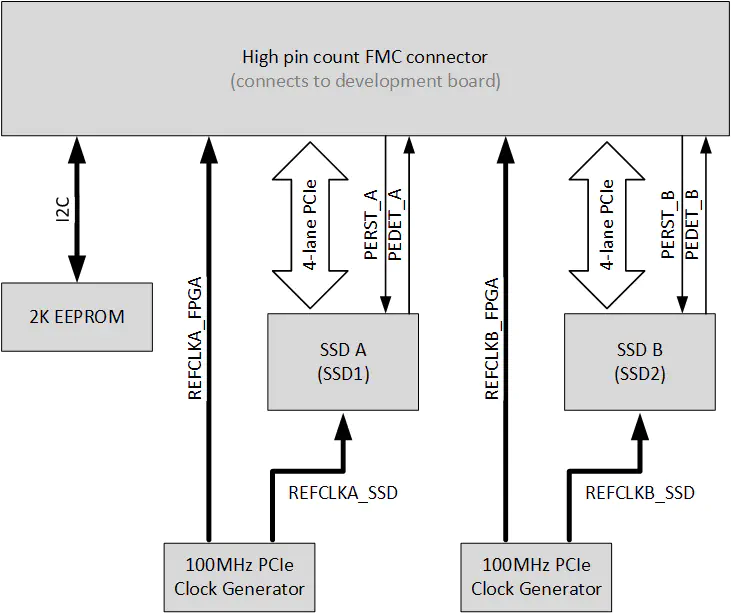
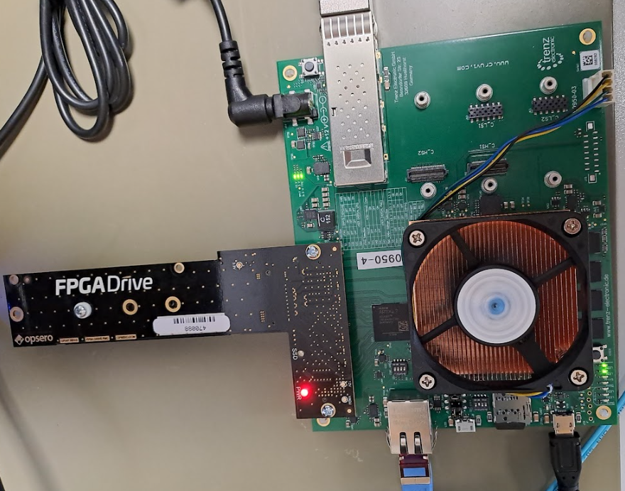
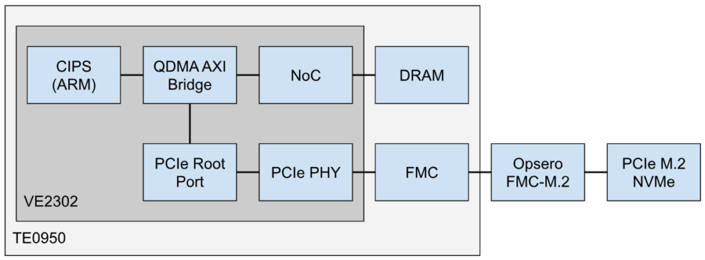
MLE’s NVMe FPGA Full System Stack facilitates connectivity between the ARM Processing System on AMD Versal AI Edge FPGAs with NVMe PCIe SSDs via the Opsero FPGA Drive FMC Gen4 card. MLE ported and validated this design to the Trenz TE0950 AMD Versal AI Edge Eval Board featuring the AMD VE2302 FPGA.
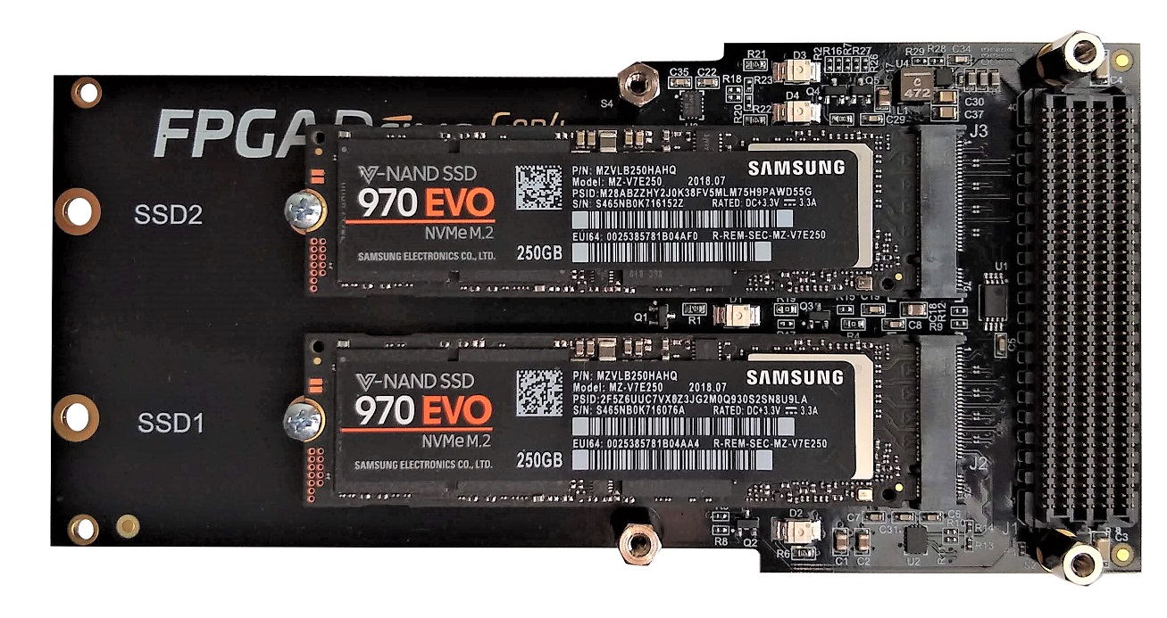
Opsero FPGA Drive
Opsero FPGA Drive FMC Gen4 is an adapter card that allows M.2 NVMe PCIe SSDs to be connected to FPGA and SoC based development boards. The adapter card uses the FPGA Mezzanine Card (FMC) form factor for connection with FPGA and SoC development boards via the FMC or FMC+ connector. It has 2x M-key M.2 sockets and can carry M.2 PCIe SSDs of length 30mm, 42mm, 60mm, 80mm or 110mm. Each M.2 socket has its own independent connection to the FPGA for maximum throughput and can support a 4-lane PCIe connection up to Gen4.
AMD Versal compatibility list:
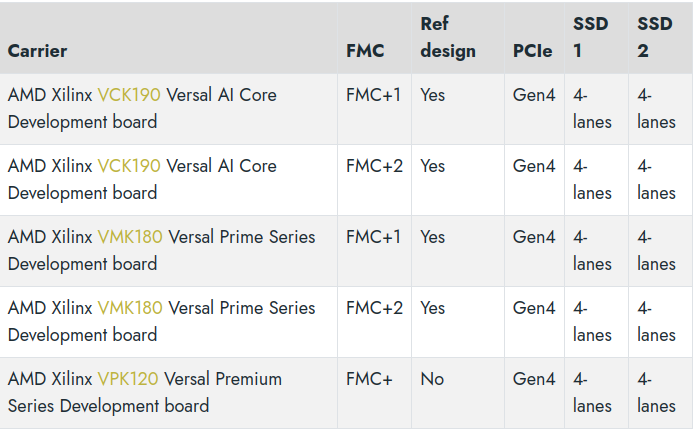
Note: MLE’s NVMe FPGA Full System Stack is validated on AMD Versal AI Egde FPGAs. Other AMD Versal FPGAs are supported upon request.
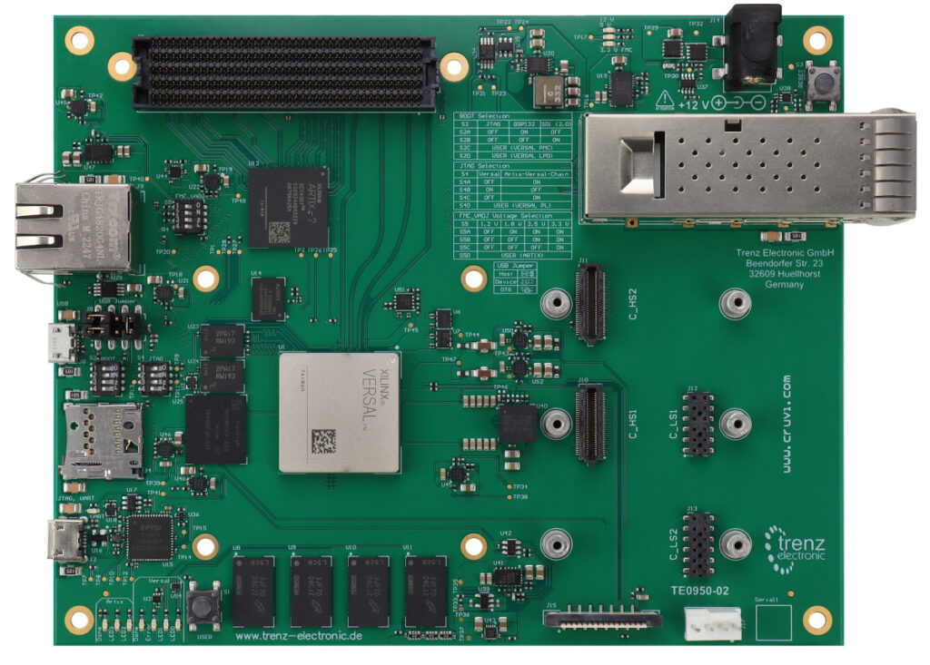
Trenz TE0950
The Trenz Electronic TE0950 is a powerful adaptive SoC evaluation board powered by AMD Versal™ AI Edge VE2302. This FPGA features the powerful processing system based on a dual-core ARM Cortex A72 and dual-core ARM Cortex R5F to deliver power-efficient embedded compute with the safety and security required for real-time systems. The dual-core Arm® Cortex®-A72 application processor is ideal for running Linux-class applications, while the dual-core Arm Cortex-R5F real-time processor handles safety-critical code for the highest levels of functional safety (ASIL and SIL).
Trenz TE0950 includes the FMC connector with 4 GTYP lanes, enabling it to support one SSD through an Opsero FPGA Drive FMC adapter card.
MLE NVMe FPGA Full System Stack on Trenz TE0950
MLE has implemented and verified the NVMe FPGA Full System Stack on the Trenz TE0950 based on existing VMK180 designs (GitHub), supporting 1x M.2 NVMe PCIe SSD only.
Hardware:
- Trenz TE0950, Rev. TE0950-3-EGBE21C, additional TE0950 Fansink
- Opsero: FPGA Drive FMC Gen4
- Samsung SSD 990 PRO 2TB, SN S6Z2NJ0W708541Y, FW Rev. 3B2QJXD7
Linux
Petalinux (6.1.30-xilinx-v2023.2 aarch64 GNU/Linux) is running on the ARM PS.
The Linux enumerated the PCIe Root Port and the PCIe NVMe device:
-[0000:00]---00.0-[01]----00.0 Samsung Electronics Co Ltd Device a80c
PCIe Root Port:
00:00.0 PCI bridge: Missing Link Electronics, Inc. Device 1000
      Capabilities: [70] Express (v2) Root Port (Slot+), MSI 00
      LnkSta:       Speed 16GT/s, Width x4
PCIe Endpoint:
01:00.0 Non-Volatile memory controller: Samsung Electronics Co Ltd Device a80c
Capabilities: [70] Express (v2) Endpoint, MSI 00
LnkSta:       Speed 16GT/s, Width x4
Relevant Linux Kernel messages:
xilinx-xdma-pcie b0000000.axi-pcie: host bridge /amba_pl@0/axi-pcie@a8000000 ranges:
xilinx-xdma-pcie b0000000.axi-pcie: No bus range found for /amba_pl@0/axi-pcie@a8000000, using [bus 00-ff]
xilinx-xdma-pcie b0000000.axi-pcie: MEM 0x00a8000000..0x00afffffff -> 0x00a8000000
xilinx-xdma-pcie b0000000.axi-pcie: PCIe Link is UP
xilinx-xdma-pcie b0000000.axi-pcie: PCI host bridge to bus 0000:00
nvme nvme0: pci function 0000:01:00.0
nvme 0000:01:00.0: enabling device (0000 -> 0002)
nvme nvme0: Shutdown timeout set to 10 seconds
nvme nvme0: 2/0/0 default/read/poll queues
The NVMe Device gets listed as Linux block device:
NAME         MAJ:MIN RM   SIZE RO TYPE MOUNTPOINTS
mmcblk1      179:0    0 119.1G  0 disk
|-mmcblk1p1  179:1    0     1G  0 part /run/media/boot-mmcblk1p1
`-mmcblk1p2  179:2    0   100M  0 part /run/media/root-mmcblk1p2
mmcblk0      179:8    0  29.1G  0 disk
mmcblk0boot0 179:16   0     4M  1 disk
mmcblk0boot1 179:24   0     4M  1 disk
nvme0n1      259:0    0   1.8T  0 disk
NVMe Info:
nvme-subsys0 - NQN=nqn.1994-11.com.samsung:nvme:990PRO:M.2:S6Z2NJ0W708541Y
\
 +- nvme0 pcie 0000:01:00.0 live
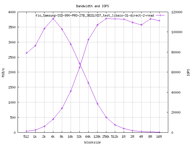
I/O Performance
For performance testing we are using the Flexible I/O Tester (FIO) – an I/O performance benchmarking utility for Linux. The diagrams below show benchmarks for data bandwidth, I/O operations per second (IOPS), Completion Latency and ARM CPU usage in PCIe Gen 4 and PCIe Gen 3.
PCIe Gen4 (16 GT/s) x4
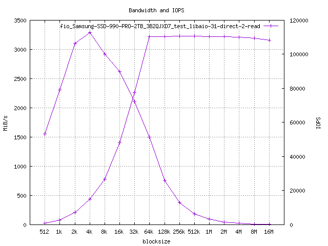
Figure 6 shows the read performance and IOPS over different block sizes at Gen4 speeds . With an IOPS maximum of about 110k at 4k block size.
Read
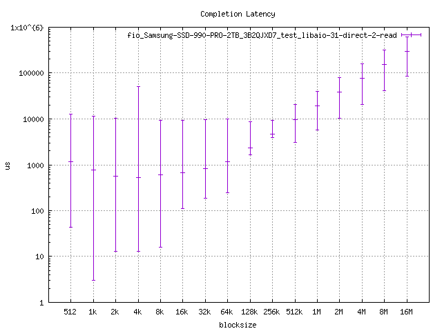
The next figure, Figure 7, shows the read completion latency, the time between read request and read response.
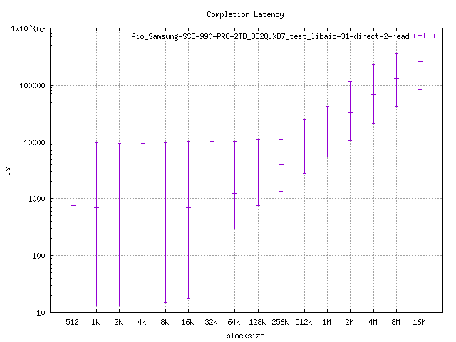
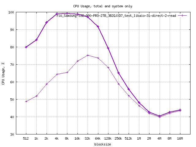
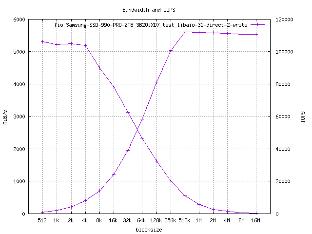
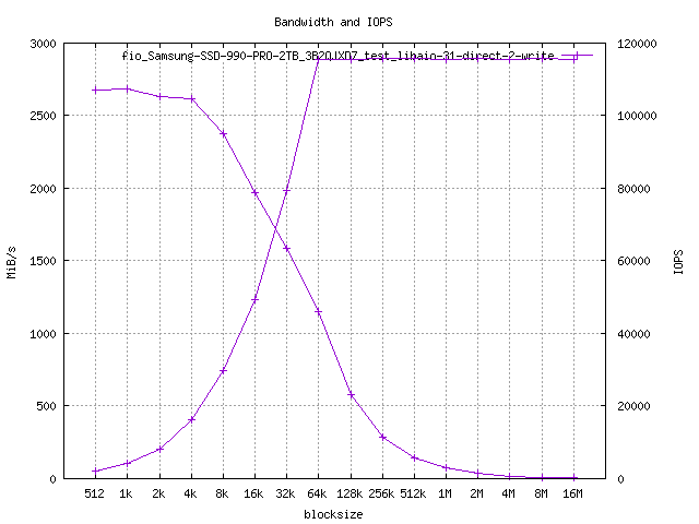
Figure 9 shows the write performance and IOPS over different block sizes. With an IOPS maximum of about 110k at 4k block size. The peak performance reaches 5600 MiB/s from the host memory to the buffer of the SSD.
Please see our other Techbriefs which explain the difference between peak and sustained performance of a SSD.
Write
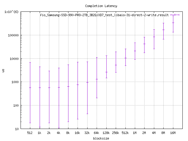
The next figure, Figure 10, shows the write completion latency, the time between write request and write response.

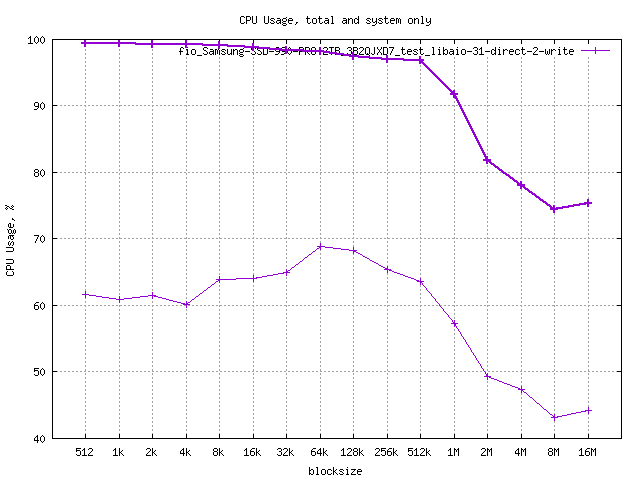
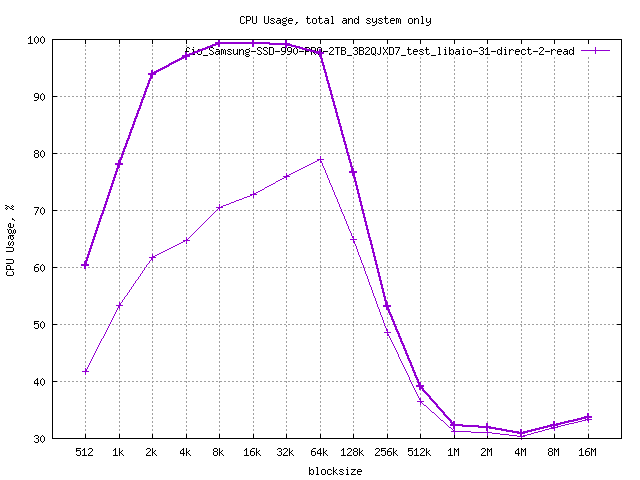
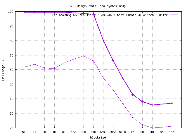
The CPU utilization, Figure 11, shows only with bigger block sizes the utilization goes down. The thin line shows the system utilization and the bold line the total CPU utilization.
PCIe Gen3 (8 GT/s) x4 Performance
Read
Figure 12 shows the read performance and IOPS over different block sizes at Gen3 speeds . With an IOPS maximum of about 110k at 4k block size. Starting from 6k block size, the link speed gets saturated.
Figure 12 shows the read performance and IOPS over different block sizes at Gen3 speeds . With an IOPS maximum of about 110k at 4k block size. Starting from 6k block size, the link speed gets saturated.
The next figure, Figure 13, shows the read completion latency, the time between read request and read response.
The CPU utilization during read is shown in Figure 14. Those numbers correlate with the IOPS, and show the nearly 100% CPU utilization at 4k block size limits the maximum IOPS. The thin line shows the system utilization and the bold line the total CPU utilization.
Write
Figure 15 shows the write performance and IOPS over different block sizes. The peak performance reaches 2900 MiB/s from the host memory to the buffer of the SSD.
Please see our other Technical Brief TB20201012 which explain the difference between peak and sustained performance of a SSD.
The next figure, Figure 16, shows the write completion latency, the time between write request and write response.
The CPU utilization, Figure 11, shows only with bigger block sizes the utilization goes down.
Conclusion
MLE’s NVMe FPGA Full System Stack shows the capabilities of the AMD Versal Processing System with an attached NVMe SSD. It is ideal for applications which require a dynamic file system and other complex storage patterns with medium write speeds.
The MLE’s NVMe FPGA Full System Stack can also be used for low-/mid-speed data logging and data recording.
Authors and Contact Information
Andreas Braun
Sr. Engineering
Missing Link Electronics GmbH
Andreas Schuler
Dir. Application
Missing Link Electronics GmbH
Yi-Ying Li
Dir. Technology Solutions
Missing Link Electronics GmbH
Missing Link Electronics GmbH
Industriestrasse 10
89231 Neu-Ulm
Germany
Missing Link Electronics, Inc.
2880 Zanker Road, Suite 203
San Jose, CA 95134, USA
🌐 www.missinglinkelectronics.com
MLE (Missing Link Electronics) is offering technologies and solutions for Domain-Specific Architectures, which focus on heterogeneous computing using FPGAs. MLE is headquartered in Silicon Valley with offices in Neu-Ulm and Berlin, Germany.