Integrated DAC for Altera Cyclone-IV Devices
This Technical Brief explains the use of Delta Sigma Modulation to implement resource-efficient Digital-to-Analog Converter (DAC) in Altera FPGA devices. Starting with an introduction into the technology of Delta Sigma Modulation, we will cover the relevant technical aspects for implementing and applying this as a flexible and cost-efficient means for DAC. We will provide the results of diligent testing using Altera Cyclone-IV FPGA devices which led to our technical specifications (Signal-to-Noise Ratios, Total Harmonic Distortion, Spurios-Free Dynamic Range values) including results for higher order modulators.
Copyright © 2026 Missing Link Electronics. All rights reserved. Missing Link Electronics, the stylized Missing Link Electronics MLE logo are the service mark and/or trademark of Missing Link Electronics, Inc. All other product or service names and trademarks are the property of their respective owners.
Field-Programmable Gate-Arrays (FPGA) are well established for implementing programmable Systems-on-Chip. A lesser known feature is their programmable digital I/O capabilities. Supporting switching at frequencies of many hundred MHz, FPGA pins have become a viable option for quality analog I/O. This Technical Brief shows how to implement Delta Sigma Digital-to-Analog Converters (DAC) inside Altera FPGA devices plus some additional passive components.
The result is a flexible integrated solution with smaller PCB footprint, field-upgradability and reduced risk of device obsolescence.
Key Features
- 78 dB SNR (compares to 14 bits effective resolution)
- Sample-rate up to 50 k samples per second
- Low Total Harmonic Distortion
- Output range 0 to 3.3 V with high linearity
- Cost-effcient for many-channel-systems
- Resource < 100 LEs for Altera Cyclone-IV
Areas of Applicability
- Audio Output
- Lighting Applications
- Motor Control
- Instrumentation and Control Systems
- Voltage Controlled Actuators
- Integrated microcontrollers with reduced risk of parts obsolescence
The integrated DAC technology presented in this Technical Brief has undergone extensive testing and diligent analysis and has demonstrated to be robust and of high quality. When combined with the appropriate design methodology it is considered application-ready.
Concept
The basic theory behind the Delta Sigma Modulation is shown in Figure 1: A 16 bit wide digital signal is the input signal and the resulting output is an oversampled and noise shaped 1 bit wide bit-stream. Inside the modulator is a feedback loop which subtracts the feedback from the input signal (delta). These differences are then summed up by the integrator (sigma).
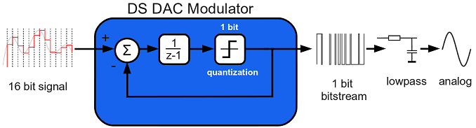
This feedback loop leads to the transfer function of the First-Order Delta Sigma Modulator: H(z)signal = 1; H(z)noise = 1 – z-1. As these functions demonstrate, the noise is high-pass filtered which is convenient looking at the other aspect of the Delta Sigma Modulation, the oversampling. With oversampling, we sample the (digital) input signal with a much higher frequency than needed by the Shannon-Nyquist theorem. The result, in combination with the high-filtering effect of the Delta Sigma Modulator is, that the noise is distributed to the higher frequencies. This is called Noise Shaping. The possible Signal-to-Noise Ratio (SNR) gain using oversampling is 3dB per octave. Using first order Delta Sigma Modulation, this SNR gain increases to 9dB per octave for a first Order Delta Sigma Modulator. The second order Delta Sigma Modulator which we also implemented has an even better gain of 15 dB per octave. These effects can be seen in Figure 2 a, b and c.
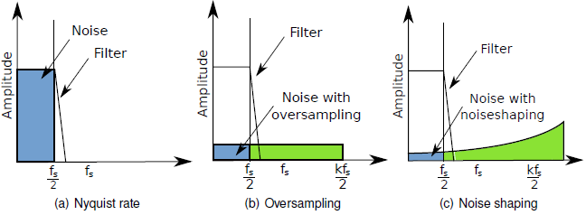
Figure 2 a) shows the Nyquist Sampling converter. All quantizing noise is in the desired signal band. The first advance is oversampling and is shown in b): It distributes the noise equally over the sample spectrum. The final improvement is Noise Shaping which is shown in c). Noise-shaping acts as a high pass for the noise.
However, the drawback of Noise Shaping is that one must come up with appropriate parameter sets to operate the inherently instable Delta Sigma Modulator.
Parameter Setting
To obtain suitable parameters for the Delta Sigma Modulator, a Matlab simulation was created. The design flow for the parameter creation can be seen in Figure 3:
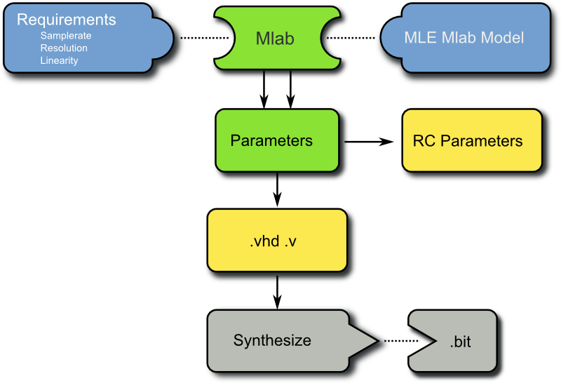
A parameter space is searched for the best results regarding Signal-to-Noise Ratio (SNR), Total Harmonic Distortion (THD) and Spurious Free Dynamic Range (SFDR). The Delta Sigma Modulator can be a first-order Delta Sigma Modulator or a 2nd-order Modulator. The steps for creating a 2nd order Delta Sigma Modulator are shown below. First the parameter space which includes the two forward coefficients and the two feedback coefficients is searched. In order to make the parameter space smaller, the two feedback and the two forward coefficients were chosen to be equal. A 3-D plot of the resulting simulation output can be seen in Figure 4.
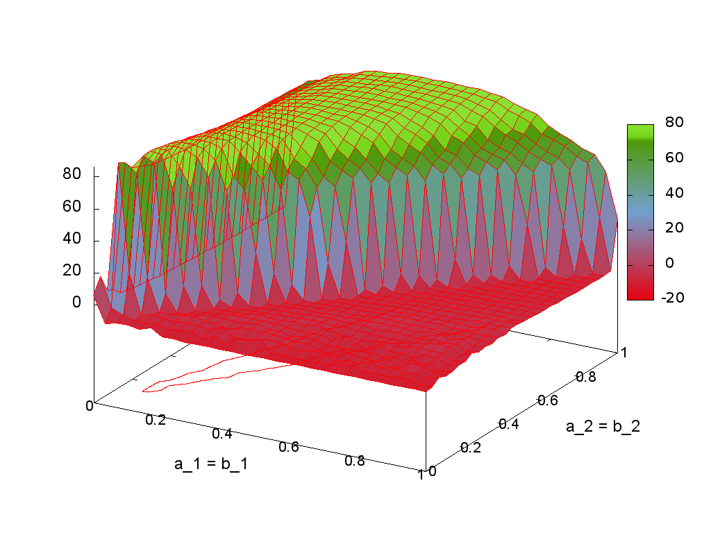
The plot shows the range of the two forward and feedback coefficients, where good results and stability with an SNR above 80 dB are expected. It also shows that above a certain threshold, the results get really bad. This is for example where the modulator gets instable.
Implementation
The basic principle is shown in Figure 5. The actual Delta Sigma Modulator is built using only FPGA logic resources for implementing the integrators, the feedback coefficients and the 1 bit comparator. The generated bit stream is fed into an output pin of the FPGA and then low-pass filtered using a RC combination, which is the only external circuitry.
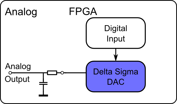
The Delta Sigma DAC was implemented using VHDL and currently runs on Xilinx and Altera FPGA’s. It consists of a second-order Delta Sigma Modulator which is implemented directly inside the FPGA. Additionally to the second-order Delta Sigma Modulator, Dithering is implemented to reduce idle tones an thus improve the SFDR and the THD. Dithering adds pseudo-random noise to the Delta Sigma Modultars feedback signal and, thereby, has a positive effect on the stability. Dithering can easily be implemented using Linear-Feedback-Shirt-Registers (LFSR), for example.
The default output voltage ranges from 0 V to the feedback pin output bank voltage (typically 3.3 V). It can be extended by using an op-amp to amplify the output signal, or by a simple transistor circuit. One can achieve high DAC quality without the need for high quality passive components for the Delta Sigma Modulator which is a benefit of this method. The only requirement is that the low-pass cut-off frequency is above the desired signal frequency but low enough to cut-off the shaped noise.
Testing
To validate the simulation results, diligent analysis was done. In particular we tested and measured the quality of results for Altera Cyclone-IV FPGA devices, namely the EP4CE115 which is located on the Terasic Industrial Networking Kit (INK) DE2-115 board. Examplary values for the resistors and the capacitor were picked from simulation, and were determined to be 80 nF for the capacitor and 100 Ohm for the resistor. These are values from the parameterization for a 20 khz cut-off frequency.
The Delta Sigma Modulator was fed with a sine signal generated by the FPGA. This signal was processed by the Delta Sigma DAC and afterwards measured with a spectrum analyzer and evaluated by Matlab. An exemplary spectrum for a 1 kHz input sine-wave signal can be seen in Figure 6
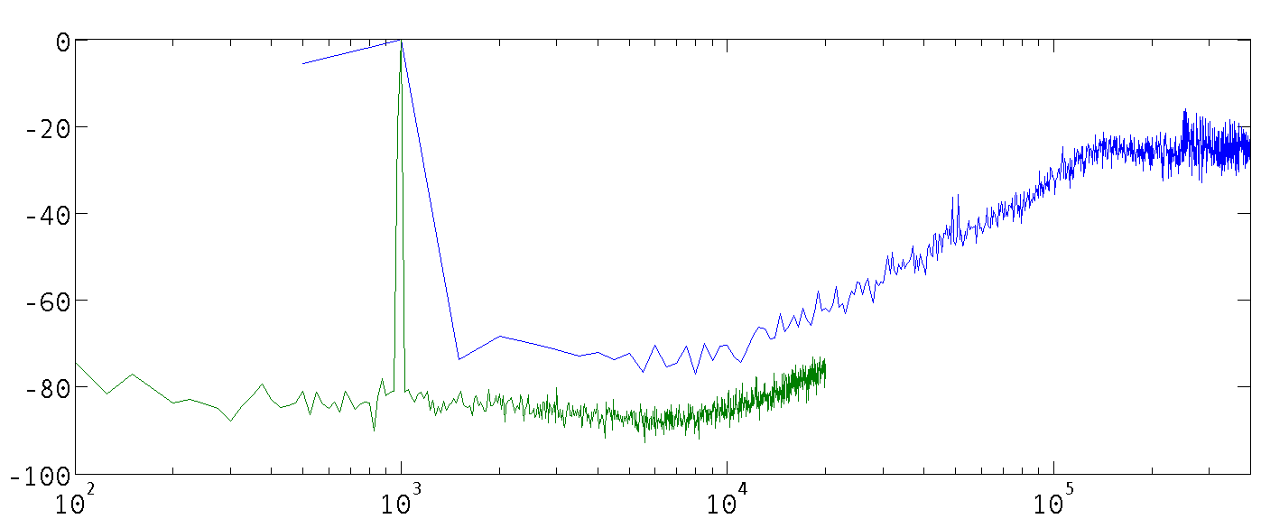
In Figure 6 you see two lines with different bandwidth settings. This was done because the spectrum analyzer has a limited measure point memory of 801 points. To visualize the effect of noise shaping two measurements were made. The lower one is from 10 to 20 kHz to see the noise in the desired spectrum. The upper one was recorded with a wider spectrum range. It shows the noise shaping of a second order Modulator where the noise is shaped with 40 dB per octave.
Quality of Results
The important parameters of an DAC are the SNR, the THD and the SFDR. These parameters have been measured using a 1 kHz sine tone input, and the sample-frequency of the bit-stream was chosen to be 10 MHz. The resulting SFDR is 78 dB, which can also be seen in Figure 6.
We also tested different configurations of the Delta Sigma Modulator: A first-order Delta Sigma Modulator with and without Dithering and a second-order Modulator. These were measured with an 1 kHz input signal with an amplitude of up to 0.5 times the maximum amplitude (determined by the maximum input voltage of 3.3 V). These results are shown in Table 1.
| Architecture | SNR | THD |
|---|---|---|
| First-Order DSM | 49.4 dB | 56.1dB |
| First-Order DSM with Dithering | 47.8 dB | 59.1dB |
| Second-Order DSM | 58.5 dB | 63.7 dB |
The table shows that Dithering adds a little noise to the SNR but at the same time improves the stability of the Delta Sigma Modulator, and thereby, the THD. It also shows the improvement in both SNR and THD when a higher order modulator is used. It should be mentioned that the second order modulator has the disadvantage of a limited input range because of the inherent instabilities.
Resource Requirements
The resource usage of the particular FPGA design used in the Altera Cyclone-IV EP4C115 FPGA device is shows in Table 2. As additional I/O resources 1 LVTTL pin per DAC channel is needed.
| Architecture | LEs |
|---|---|
| First-Order DSM | 22 |
| First-Order DSM with Dithering | 41 |
| Second-Order DSM | 87 |
Application – Class S Amplifier
The bitstream which is generated by the FPGA can also be used to drive higher loads by using a half or full-bridge. The result is for example an Class S Amplifier and can be used to drive motors in electromobility applications or high power speakers. The benefits of this usage over PWM, for example, is the better SNR and THD which results for example in lower EMI. An example application circuit can be seen in Figure 7.
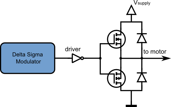
Another benefit is the possibility to compensate for the non-linearities of the switching circuitry, for example the capacity of the transistor gate by adding it to the prior parameterization.
Reference
[1] ORTMANNS, M. Personal Communication. 2010.
[2] SCHUBERT, E., ZEKEL, H., GRUMBEIN, C., AND ZIMMERMANN, A. FPGA can do analog! Embedded World 2011 (2011).
[3] SOUSA, F., MAUER1, V., DUARTE, N., JASINSKI, R. P., AND PEDRONI, V. A. Taking advantage of LVDS input buffers to implement sigma-delta A/D converters in FPGAs. IEEE, 2004.
🌐 www.missinglinkelectronics.com
MLE (Missing Link Electronics) is offering technologies and solutions for Domain-Specific Architectures, which focus on heterogeneous computing using FPGAs. MLE is headquartered in Silicon Valley with offices in Neu-Ulm and Berlin, Germany.