Connecting FPGA Companion Chips to Intel ATOM CPUs
This Technical Brief introduces the options for connecting Field-Programmable Gate-Array (FPGA) devices via Peripheral Component Interconnect Express (PCIe) to microprocessors such as the Intel ATOM microprocessor. Using FPGAs as companion chips adds flexibility to implement special-purpose I/O and efficient means for parallel and digital signal processing.
On the hardware side, we will describe the design options when using Altera Arria GX or Xilinx Virtex-5 devices. On the software side, we compare the performance of polling interfacing with Direct Memory Access (DMA) running under Linux.
Copyright © 2026 Missing Link Electronics. All rights reserved. Missing Link Electronics, the stylized Missing Link Electronics MLE logo are the service mark and/or trademark of Missing Link Electronics, Inc. All other product or service names and trademarks are the property of their respective owners.
The ability to connect Field Programmable Gate-Array (FPGA) technology as companion chips to microprocessors opens the world of Application Specific Standard Processing (ASSP) to embedded systems designers. ASSP offers many advantages for implementing electronic systems:
First, it provides flexibility to implement that particular special-purpose I/O connectivity that your microprocessor and/or micro-controller may not have. For example, certain automotive and/or industrial I/O such as CAN, FlexRay, MOST, SerCos, Profibus, Ethercat, etc are typically not provided by many general purpose processors but can easily be implemented in an FPGA companion chip – an aspect which is illustrated by the GENIVI Alliance’s computing platform [GENIVI] or the Intel Industrial Control Reference Design [Intel]. Using Sigma-Delta converters, FPGAs can even be used to provide integrated analog-to-digital or digital-to-analog connectivity to an embedded system.
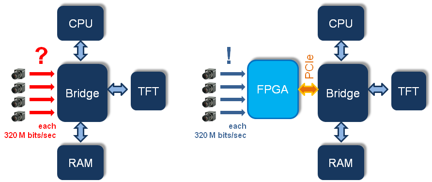
Second, the FPGA compute fabric offers powerful means for parallel processing and digital signal processing, as it is, for example, required by video image stream processing in automotive driver assist systems and in machine visioning applications. Also, parallel processing in the FPGA fabric sometimes is more advantageous for implementing real-time behavior compared to software running in a Real-time Operating System (RTOS).
This makes system implementation more efficient and allows to scale a platform’s compute performance with the application’s needs.
Therefore, it is important to manage the communication between the FPGA devices and the microprocessors. When designing with embedded microprocessors (i. e. embedded inside the FPGA), things are straight-forward because of the tools and support by the FPGA vendors. In case of Altera devices, one or more NIOS II soft CPU cores can be connected to the FPGA fabric via the so-called Avalon bus. The entire design flow is facilitated by Altera’s SOPC Builder tool suite.
In case of Xilinx devices two choices exist, depending on the microprocessor: One or more soft microprocessor cores, so-called MicroBlaze, can be integrated or one or more embedded PowerPC cores (available in the Virtex-4 FX and the Virtex-5 FXT devices). Connectivity is provided via the Processor Local Bus (PLB). The design flow is facilitated by the Xilinx EDK tool suite.
In those cases the entire system – custom hardware implemented in the FPGA fabric and the microprocessor running software – can be verified while running inside a simulator (for example, Mentor Graphics ModelSim). Such co-simulation of hardware and software makes system-level verification and debugging easy and efficient.
Things get more complicated when external buses on a printed circuit board are used.
State-of-the-art for such connectivity is the Peripheral Component Interconnect Express (PCIe) bus. PCIe was introduced in 2004 by the Intel Corporation to replace the older PCI and AGP standards. The theoretical bandwidth of a single-lane PCIe connect in version 1.0 is 250 MB/sec. Today, it is not only ubiquitous in personal computers but it is also an important choice for compute intensive embedded systems.
While in the “old days” of PCI a special PCI chipset was needed for connectivity most of today’s FPGA devices have dedicated, built-in hard macros for PCIe connectivity. Some FPGAs even have dedicated PCIe endpoints such as the Altera Arria II GX device or the Xilinx Virtex-5 and Virtex-6 devices. As a result, the design challenges have moved from hardware printed circuit board design to finding the proper system architecture in the FPGA and in developing the software infrastructure for PCIe connectivity between the microprocessor and the FPGA companion.
Because of the exciting possibilities to build powerful and cost-efficient systems, here at Missing Link Electronics we have looked more closely into the various options for PCIe connectivity using FPGAs. Over the next pages we like to share some of the findings with you to help you jump start your PCIe-based design.
We will be describing the two software interfacing concepts for PCIe, polling and interrupt-driven communication using Direct Memory Access (DMA), as well as design starting points for the two dominant FPGA device vendors, Altera and Xilinx.
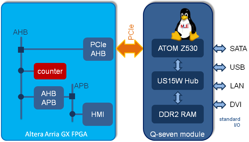
For this experiment an Altera Arria GX device (more precisely the Altera EP1AGX90E-F1152) was connected to a so-called Qseven [Qseven] computer-on-module. The Qseven module comprised the Intel ATOM Z530PT microprocessor with 1.2 GHz and the Intel US15W System Controller Hub which provides the PCIe connectivity.
The foundation of this experiment was the Industrial Reference Platform from Gleichmann Electronics Research [HPE IRP]. The example design used the PCIe Endpoint and the PCIe-to-AMBA-Bridge IP core to interconnect an Advanced High-performance Bus (AHB) with the PCIe bus of the Qseven module. Another AHB-to-APB-Bridge connects an examplary IP core to the system’s Human-Machine-Interface (HMI) which controls some general-purpose I/Os for example, LEDs and buttons). Our experimental design was built with Gleichmann’s Hpe_desk/AMBA-IP-Manager.
To get a feeling for the robustness, performance and the design effort when extending this PCIe solution we added a 32-bit counter as a data source to the FPGA design. We then developed a simple polling PCIe driver and integrated it into the FPGA-focused Missing Link Electronics Linux which was running on the Intel ATOM microprocessor.
While the hardware counter inside the FPGA incremented by one at 100 MHz the PCIe polling driver on the microprocessor was reading this counter value through the PCIe connectivity as fast as possible (basically, the polling driver was a for-loop of ioread32 function calls). This experiment was very quickly implemented and ran reliably without any glitches. On average, the polling driver read every 150th count. The read-to-increment ratio was very consistent and deterministic and can roughly be translated into a read transfer rate of 2.5 MB/sec. Again, the purpose of this experiment was not to build a powerful system but to give a feeling for the FPGA-to-microprocessor environment from a system-level perspective.
The previous experiment encouraged us to test for more by extending the hardware setup from above, the Qseven module plus the Altera Arria GX FPGA companion, with a high-performance connectivity using Direct Memory Access (DMA) transfers.
As a starting point for this experiment we selected the PCI Express High Performance Reference Design which is sometimes called the “Chaining DMA Reference Design” as it is described in the Altera Application Note 456 [AN456]. This reference design can serve as a great starting point for high-performance designs because it implements chaining DMA transfer and scatter-gather DMA transfer modes. While it comes as a Quartus II design, so you cannot take advantage of the powerful SOPC Builder tool, it includes C source code for the PCIe device drivers for Windows and for the Linux mainline kernel.
The High Performance Reference Design is a plain Quartus II design, which directly connects a DMA controller to the PCIe bus. In its original state the DMA controller has some BRAM connected to it, which can be read and written by a host processor through the DMA controller. We modified this design by disconnecting the write side of the DMA controller and instead connect a simple counter to the BRAM. Thereby, the BRAM was continuously filled (i.e. via repeated wraparound) with predetermined counter values.
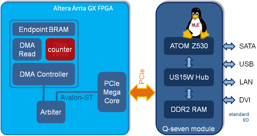
This FPGA design for PCIe is special because it does not contain any PCIe-to-other-bus bridges. Instead a BRAM is directly connected to the PCIe endpoint. Therefore the BRAM can serve as a data transfer cache to the microprocessor – an architecture which easily can be extended, for example to machine visioning applications where the BRAM operates as a frame buffer for cameras.
For our tests, the software for PCIe data transfer acted like most other DMA device driver software: It first sets up a DMA transfer by programming the DMA controller inside the FPGA to read 16 KB of BRAM data as a block and to store it into a particular location of the ATOM system’s memory. Then the driver waits for completion of the transfer which is denoted by a software interrupt.
Because we used the Linux kernel for this experiment performance analysis was as easy as checking the timestamps of the kernel debug messages of printk (technically, this is not a very precise measurement but an appropriate fast path for checking timing / performance). To analyze the robustness of this system and to verify that no data corruption had occurred, we checked that the received data matched the BRAM data as it was initiated by the BRAM counter.
This quick-to-implement performance measuring suggested data transfer rates of approximately 170 MB/sec for transferring the 16 KB blocks of data. So, in real life, you can expect data transfer rates well above 100 MB/sec which makes this FPGA-to-microprocessor connectivity applicable to bandwidth demanding applications such as multi-camera systems.
On another occasion we had the opportunity to evaluate the PCIe connectivity between a Xilinx Virtex-5 device (more precisely the Xilinx XC5VFX70T on the Xilinx ML507 evaluation board) and a dual-core 1.6 GHz Intel ATOM 330 microprocessor host system using the NVIDIA MCP7A-ION chipset. The two hardware systems, the Xilinx ML507 evaluation board and the microprocessor host system, were connected via a single-lane PCIe. On the host system we were running our Missing Link Electronics Embedded Linux.
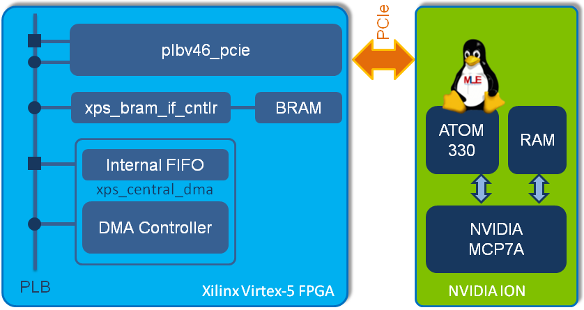
The foundation for our experiments was the Xilinx Application Note 1040 [XAPP1040] which is addressing PCI Express connectivity for the Xilinx ML507 evaluation board. This describes the block diagram of this reference system:
The XAPP 1040 design was built with Xilinx EDK toolsuite and had a PLB-to-PCIe-Bridge to connect PLB device IP cores to the PCIe bus. A first PLB master device was the Central DMA Controller, the second PLB slave device a BRAM controller connected to 64 KB of BRAM. Depending on the configuration the PLB-to-PCIe-Bridge allows to translate bus accesses to certain address ranges in either direction.
The BRAM was initialized with predetermined values from within the Xilinx EDK toolsuite using a simple standalone application which comes with XAPP 1040 (on the side, this standalone application can also be used for analyzing the PLB-to-PCIe-Bridge via the ML507’s RS232 debug port). So the contents of the BRAM was known. While the Central DMA Controller of this reference design does not support scatter-gather DMA transfers it is quite powerful and can easily be extended because of the use of the PLB and its integration into the Xilinx EDK tool suite. For example, different bus bridges can be added to connect additional hardware blocks to PCIe via the On-chip Peripheral Bus (OPB) or via the Wishbone bus.
In a first experiment we tested a simple PCIe polling data transfer from the 64 KB BRAM. The polling software was derived from a common Linux kernel module for PCI / PCIe read transfer and transferred 64 KB of data from the FPGA’s BRAM into the Intel ATOM system’s memory We used the Linux ktime API as a simple to implement method for measuring the data transfer rate between the FPGA and the Intel ATOM microprocessor system. Compared to the previously used printk method the ktime API is more precise. 64 KB of data could be transferred within approximately 28.4 milliseconds which translates into a data transfer rate of approximately 2.2 MB/sec.
The second experiment for PCIe connectivity of a Xilinx Virtex-5 FPGA was using the full functionality of interrupt-based DMA transfer. By modifying the reference design we made the Central DMA controller’s control registers and the PCIe Bridge’s control registers on the PLB side accessible to the microprocessor host system – through the PCIe Bridge itself. The test software – a Linux kernel module running on microprocessor host system allocated 64 KB of system memory, configured the PCIe Bridge to make this block accessible from the PLB side of the bridge and commanded the Central DMA controller to transfer the contents of the 64 KB of PLB-hosted BRAM into the previously allocated host system’s memory.
Again we used Linux ktime API for measuring the data transfer performance. The data transfer rate peaked at approximately 160 MB/sec while sustained long-term average data transfer performance always was above 100 MB/sec.
As mentioned above, goal of those experiments was not to build a powerful system but to get a system-level understanding for PCIe as a FPGA-to-microprocessor connectivity solution.
Complementing a microprocessor system with an FPGA companion chip to provide custom peripherals and parallel signal processing is easy to implement and very robust when using PCIe. Especially in combination with embedded microprocessors such as the Intel ATOM microprocessor this offers exciting possibilities for the design of performance embedded systems.
Modern FPGA devices with their built-in PCIe support (either as hard or as soft macros) significantly reduce the hardware and printed circuit board design complexity. The reference designs from the FPGA vendors can serve as great starting points for such PCIe based designs.
Utilizing the Linux operating system embedded systems designers can take control over the entire system stack. One can easily add device drivers for custom PCIe peripherals by adjusting other PCIe device drivers. Plenty of examples for PCI and PCIe devices are readily available from the open source community.
100 MB/sec or more data transfer rates between the system memory and the FPGA companion chips can be achieved which offers great optimization potential for hardware – software partitioning of compute intensive embedded systems.
References
[GENIVI] GENIVI Alliance: GEVINI Alliance Fact Sheet, March 2009.
http://at.projects.genivi.org/wiki/
[Intel] Intel Corporation: Intel Industrial Control Reference Design Embedded Computing, 2009.
http://intel.com/go/industrial
[Qseven] Qseven Consortium: Qseven Specification Revision 1.11, 2009.
http://www.qseven-standard.org
[HPE IRP] Gleichmann Electronics Research: Industrial Reference Platform for Intel ATOM, 2009.
http://www.ge-research.com/intel_industrial_platform.html
[AN456] Altera Corporation: AN-456-1.2: PCI Express High Performance Reference Design, August 2009.
http://www.altera.com/literature/an/an456.pdf
[XAPP1040] Xilinx, Inc.: Reference System: PLBv46 Endpoint Bridge for PCI Express in a ML507 Embedded Development Platform, January 5th, 2009.
http://www.xilinx.com/support/documentation/ml507.htm
🌐 www.missinglinkelectronics.com
MLE (Missing Link Electronics) is offering technologies and solutions for Domain-Specific Architectures, which focus on heterogeneous computing using FPGAs. MLE is headquartered in Silicon Valley with offices in Neu-Ulm and Berlin, Germany.