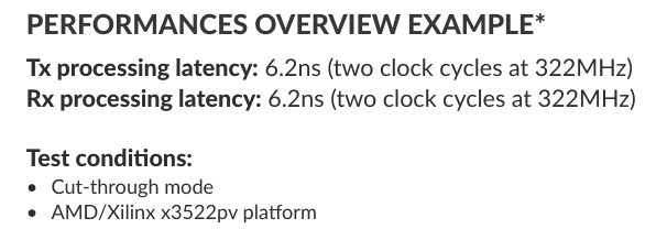
Myth-Busting Latency Numbers for TCP Offload Engines
When you shop around for a TCP IP-Core for TCP offload engines, don’t you ask yourself: What does that really mean when you see numbers like this?
This Technical Brief sheds light on TCP/IP processing in an FPGA, and in particular busts some myths about latency numbers. Here, we will describe proper ways of measuring latency numbers, and why latency numbers do matter for TCP offload engines when implementing TCP/IP in FPGAs.
Based on MLE’s past projects experience, it all comes down to technical and economical feasibility determined by FPGA resource costs!
Shift-Left Your FPGA Design Projects
Summary
FPGA Full System Stacks comprising off-the-shelf FPGA System-on-Modules (SoM) plus pre-validated FPGA IP Cores and subsystems can greatly accelerate the time-to-market of your FPGA design project. Advantages of FPGA Full System Stacks include:
- FPGA developers can rely on a tested and verified subsystem implementation. The concept of re-use increases design productivity while sharing the FPGA subsystem development costs and risks over many users.
- Pre-validated FPGA IP-Cores and subsystems make clever use of the different FPGA resources to realize a cost/performance optimized domain-specific architecture.
- Software is included in the form of kernel space device drivers, user-space programmer APIs, and sometimes even complete OS images, all nicely tuned for guaranteeing the overall system’s reliability and performance.
FPGA Full System Stacks from MLE are integrated with select FPGA SoMs from Trenz Electronics and are focused on applications such as:
- Realiable, Low-Latency, High-Throughput Network Transports
- High-Speed Data Acquisition
- Augmented Stereo Computer Vision
- High-Speed Data Record & Replay
We describe a design methodology using FPGA Full System Stacks and share our experiences from real customer designs.
- Shift-Left Your FPGA Design Projects
- Summary
- Shift-Left Your FPGA Design Projects
- 1. Benefits of FPGA System-on-Modules
- 2. Advantages of Pre-Validated FPGA Subsystems
- 2.1. NPAP – MLE’s Network Protocol Acceleration Platform
- 2.2. High-Speed Data Acquisition
- 2.3. Augmented Stereo Computer Vision
- 2.4. High-Speed Data Record & Replay
- 3. A Shift-Left Methodology for FPGA Design
- 3.1. First Step: Development Kits for Architecture Validation
- 3.2. Ship Products based on SoMs
- 3.3. Cost-Down for Volume Ramp-Up
- 4. Real-Life Examples of Shift-Left FPGA Design
- 4.1. From Devkit to SoM to First-Customer-Ship
- 4.2. From SoM to Chip-Down
- 4.3. From SoM to PCIe Card
- 5. Conclusion
High-Speed Data Acquisition Systems
Challenges and design choices to network FPGAs and servers for high-speed data acquisition or retrieval. We discuss TCP/IP as a very fast transport when using TCP/IP full accelerators, in the sensor-side FPGA and in the server.
- High-Speed Data Acquisition Systems
- 1 Challenges in High Speed Data Acquisition
- 2 Design Choices for High Speed Data Acquisition
- 2.1 TCP/IP Full Acceleration for High Speed Data Acquisition
- 2.2 Optimize the Server’s Network Subsystem
- 2.3 Use Offload Engines, Kernel Bypass, or RDMA for High Speed Data Acquisition
- 2.4 Use an FPGA NIC with TCP/IP Full Acceleration for High Speed Data Acquisition
- 2.5 Use PCIe Peer-to-Peer for High Speed Data Acquisition
Put a TCP/UDP/IP Turbo Into Your FPGA-SmartNIC
How MLE and Fraunhofer HHI are breaking the 500 MHz fMax barrier in network protocol acceleration (TCP/IP stack) by using Intel Agilex FPGAs as an FPGA SmartNIC.
Summary
MLE provides full system stacks including FPGAs, with a focus on networking for HPC, datacenter, or telecommunications. Often, we implement so-called full accelerators where almost all protocol processing runs efficiently within the FPGA fabric.
Within this Technical Brief we elaborate on two key aspects for FPGA-based SmartNICs:
- How to implement rapid, reliable connectivity from edge to cloud using FPGA-based SmartNICs with TCP/IP stack acceleration, and
- how these implementations can benefit from modern FPGA technology, namely Intel HyperFlex, to deliver better performance, cost and power.
Our design choices for FPGA SmartNICs include the Corundum project, an open-source, high-performance FPGA-based Network Interface Card (NIC) platform. Corundum supports In-Network Processing for which we have integrated MLE’s Network Protocol Accelerator Platform (NPAP) based on the TCP/UDP/IP Full Accelerator from Fraunhofer HHI.
To enable network protocol processing at linerates of 100 Gbps, or faster, we have optimized this implementation for Intel HyperFlex architecture. The result is a “turbo charged” FPGA SmartNIC which combines several advantages:
- NPAP with high throughput for those “heavy” TCP data streams which make up for most of the network traffic.
- NPAP for those latency sensitive TCP connections where TCP round-trip time (RTT) may dominate the entire system’s response time.
- Corundum processing in open-source Linux software for the rest, i.e. all those administrative and control TCP connections which hardly use any bandwidth and which are not latency sensitive.
- Performance optimizations utilizing Intel HyperFlex to break the 500 MHz fMax barrier and to avoid FPGA resource “bloat”1.
Increase Speed and Save Resources with Simple Coding Style Changes
FPGA Programming – Increase Speed and Save Resources with Simple Coding Style Changes Table of ContentsFPGA Programming – Increase Speed and Save Resources with Simple Coding Style ChangesASIC vs. FPGA in Process AccelerationMLE Smart Process Redesign in FPGA Programming for Resource Saving and Speed Increasing ASIC vs. FPGA in Process Acceleration Compared to ASICs, FPGAs are a much more versatile option when it comes to accelerating processes with hardware, as an FPGA can be reconfigured and programmed as often as needed. However, one large benefit to ASICs is the possible maximum clock speed that can be reached. As its circuit is optimized for its specific function, it has a smaller footprint, resulting in a faster maximum clock speed. So one aspect of accelerating a process with FPGAs is not only just to redesign that process in hardware and hoping for faster results, but to smartly redesign that process to use as little hardware space as possible, resulting in a higher maximum clock speed. As engineers we know, there is always room for improvement, so we at Missing Link Electronics strive to continuously improve our existing product lineup. MLE Smart Process Redesign in FPGA Programming for Resource Saving and Speed Increasing In one of these development cycles, we encountered a simple, yet veryLatency Measurement of 10G/25G/50G/100G TCP-Cores using RTL Simulation
Latency Measurement of 10G/25G/50G/100G TCP-Cores using RTL Simulation
Distributed Systems-of-Systems which, for example, connect smart sensor hubs with centralized processing via Ethernet, require very low transport latencies in order to deliver short response times. This makes it difficult for system designers to evaluate. And, things get worse if the measurement setup and methodology is not clearly explained, neither can be reproduced. Therefore, in this Technical Brief we describe how we use the Questa Advanced Simulator from Siemens EDA to measure network latency and analyze latency in a network protocol processing system. And, we also provide the most recent latency values for NPAP, the TCP/IP Stack from Fraunhofer HHI which is, as it turns out, very competitive with other solutions. Being integrators ourselves, we believe we owe this to the FPGA ecosystem!